Rev. 4106F≠8051≠10/02
Features
∑
MPEG I/II-Layer 3 Hardwired Decoder
≠ Stand-alone MP3 Decoder
≠ 48, 44.1, 32, 24, 22.05, 16 kHz Sampling Frequency
≠ Separated Digital Volume Control on Left and Right Channels (Software Control
Using 31 Steps)
≠ Bass, Medium, and Treble Control (31 Steps)
≠ Bass Boost Sound Effect
≠ Ancillary Data Extraction
≠ "CRC Error" and "MPEG Frame Synchronization" Indicators
∑
Programmable Audio Output for Interfacing With Common Audio DAC
≠ PCM Format Compatible
≠ I
2
S Format Compatible
∑
8-bit MCU C51 Core Based (F
MAX
= 20 MHz)
∑
2304 Bytes of Internal RAM
∑
64K Bytes of Code Memory
≠ Flash: AT89C51SND1C, ROM: AT83C51SND1C
∑
4K Bytes of Boot Flash Memory (AT89C51SND1C)
≠ ISP: Download from USB or UART to Any External Memory Cards
∑
USB Rev 1.1 Controller
≠ "Full Speed" Data Transmission
∑
Built-in PLL
≠ MP3 Audio Clocks
≠ USB Clock
∑
MultiMedia CardTM Interface Compatibility
∑
Atmel DataFlash
Æ
SPI Interface Compatibility
∑
IDE/ATAPI Interface
∑
2 Channels 10-bit ADC, 8 kHz (8-True Bit)
≠ Battery Voltage Monitoring
≠ Voice Recording Controlled by Software
∑
Up to 44 bits of General-purpose I/Os:
≠ 4-bit Interrupt Keyboard Port for a 4 x n Matrix
≠ SmartMediaTM Software Interface
∑
Standard Two 16-bit Timers/Counters
∑
Hardware Watchdog Timer
∑
Standard Full Duplex UART with Baud Rate Generator
∑
Two Wire Interface (TWI) Master and Slave Modes Controller
∑
SPI Master and Slave Modes Controller
∑
Power Management
≠ Power-on Reset
≠ Software Programmable MCU Clock
≠ Idle Mode, Power-down Mode
∑
Operating Conditions:
≠ 3V,
±
10%, 25 mA Typical Operating at 25∞C
≠ Temperature Range: -40
∞
C to +85
∞
C
∑
Packages
≠ TQFP80, PLCC84 (Development Board)
≠ Dice
Description
The AT8xC51SND1C are fully integrated stand-alone hardwired MPEG I/II-Layer 3
decoders with a C51 microcontroller core handling data flow and MP3-player control.
The AT89C51SND1C includes 64K Bytes of Flash memory and allows In-System Pro-
gramming through an embedded 4K Bytes of Boot Flash Memory.
Single-Chip
Microcontroller
with MP3
Decoder and
Man-Machine
Interface
AT83C51SND1C
AT89C51SND1C
Preliminary
Summary

2
AT8xC51SND1C
4106F≠8051≠10/02
The AT83C51SND1C includes 64K Bytes of ROM memory.
The AT8xC51SND1C includes 2304 Bytes of RAM memory.
The AT8xC51SND1C provides all necessary features for man machine interface like
timers, keyboard port, serial or parallel interface (USB, TWI, SPI, IDE), ADC input, I
2
S
output, and all external memory interface (NAND or NOR Flash, SmartMedia, MultiMe-
dia, DataFlash cards).
Typical Applications
∑
MP3 Player
∑
PDA, Camera, Mobile Phone MP3
∑
Car Audio/Multimedia MP3
∑
Home Audio/Multimedia MP3
4
AT8xC51SND1C
4106F≠8051≠10/02
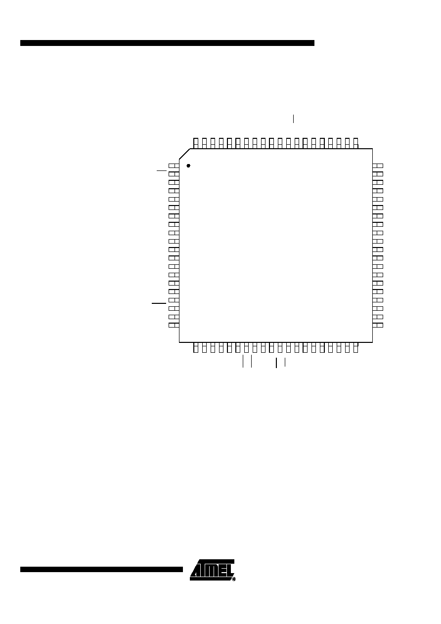
Figure 2. AT8xC51SND1C 84-pin PLCC Package
(1)
Note:
1. Only samples for development board.
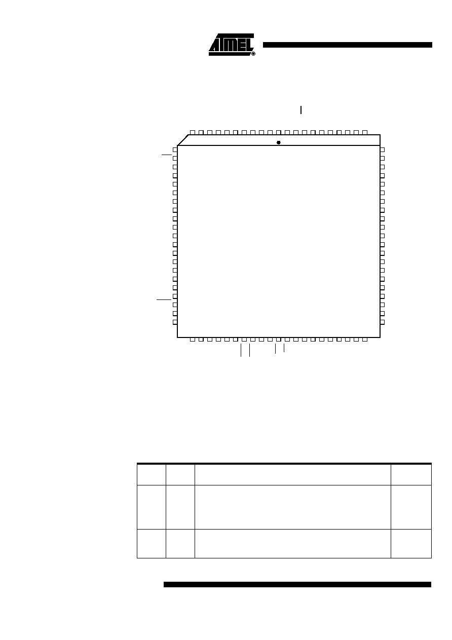
Pin Descriptions
All AT8xC51SND1C signals are detailed by functionality in Table 1 through Table 14.
AT89C51SND1C-SR (Flash)
P0
.3
/
A
D
3
P0
.4
/
A
D
4
P0
.5
/
A
D
5
VSS
V
DD
P0
.6
/
A
D
6
P0
.7
/
A
D
7
P2
.0
/
A
8
P2
.1
/
A
9
P
3
.3
/IN
T
1
P
3
.4
/T
0
P
3
.5
/T
1
P
3
.6
/W
R
P
3
.2
/IN
T
0
65
64
63
62
61
60
59
58
55
56
57
12
13
14
15
16
17
22
20
19
33
34
35
36
37
4
3
2
1
84
83
82
81
80
79
78
NC
P2.3/A11
P2.4/A12
P2.6/A14
P2.5/A13
P2.7/A15
MCLK
MDAT
MCMD
P0
.2
/
A
D
2
P0
.1
/
A
D
1
P5
.0
PAVSS
VSS
X2
NC
X1
P
3
.1
/T
XD
18
21
23
24
25
38
39
40
41
42
69
68
67
66
70
5
6
7
8
9
P4
.3
/
S
S
P4
.2
/
S
C
K
P4
.1
/
M
O
S
I
P4
.0
/
M
ISO
VSS
V
DD
RST
SCLK
DSEL
DCLK
DOUT
AIN
1
AIN
0
AR
EF
N
AR
EF
P
AV
S
S
A
V
DD
VS
S
V
DD
P
3
.7
/RD
P3
.
0
/R
XD
P1.0/KIN0
P1.1/KIN1
P1.2/KIN2
P1.3/KIN3
P1.4
P1.5
P1.7/SDA
FILT
PA
V
DD
V
DD
P1.6/SCL
26
43
TST
P5
.
2
P0
.0
/
A
D
0
77
P2.2/A10
54
ALE
ISP
NC
P5
.1
P4
.7
P4
.6
76
75
10
11
28
27
29
30
31
32
U
V
DD
UVSS
44
45
46
47
48
49
50
51
52
53
74
73
72
71
P4.4
P4.5
V
DD
VSS
D-
D+
NC
P5
.
3
Table 1. Ports Signal Description
Signal
Name
Type
Description
Alternate
Function
P0.7:0
I/O
Port 0
P0 is an 8-bit open-drain bi-directional I/O port. Port 0 pins that have 1s
written to them float and can be used as high impedance inputs. To
avoid any parasitic current consumption, floating P0 inputs must be
polarized to
V
DD
or V
SS
.
AD7:0
P1.7:0
I/O
Port 1
P1 is an 8-bit bi-directional I/O port with internal pull-ups.
KIN3:0
SCL
SDA
5
AT8xC51SND1C
4106F≠8051≠10/02
P2.7:0
I/O
Port 2
P2 is an 8-bit bi-directional I/O port with internal pull-ups.
A15:8
P3.7:0
I/O
Port 3
P3 is an 8-bit bi-directional I/O port with internal pull-ups.
RXD
TXD
INT0
INT1
T0
T1
WR
RD
P4.7:0
I/O
Port 4
P4 is an 8-bit bi-directional I/O port with internal pull-ups.
MISO
MOSI
SCK
SS
P5.3:0
I/O
Port 5
P5 is a 4-bit bi-directional I/O port with internal pull-ups.
-
Table 2. Clock Signal Description
Signal
Name
Type
Description
Alternate
Function
X1
I
Input to the on-chip inverting oscillator amplifier
To use the internal oscillator, a crystal/resonator circuit is connected to
this pin. If an external oscillator is used, its output is connected to this
pin. X1 is the clock source for internal timing.
-
X2
O
Output of the on-chip inverting oscillator amplifier
To use the internal oscillator, a crystal/resonator circuit is connected to
this pin. If an external oscillator is used, leave X2 unconnected.
-
FILT
I
PLL low pass filter input
FILT receives the RC network of the PLL low pass filter.
-
Table 3. Timer 0 and Timer 1 Signal Description
Signal
Name
Type
Description
Alternate
Function
INT0
I
Timer 0 Gate Input
INT0 serves as external run control for timer 0, when selected by
GATE0 bit in TCON register.
External Interrupt 0
INT0 input sets IE0 in the TCON register. If bit IT0 in this register is set,
bit IE0 is set by a falling edge on INT0. If bit IT0 is cleared, bit IE0 is set
by a low level on INT0.
P3.2
INT1
I
Timer 1 Gate Input
INT1 serves as external run control for timer 1, when selected by
GATE1 bit in TCON register.
External Interrupt 1
INT1 input sets IE1 in the TCON register. If bit IT1 in this register is set,
bit IE1 is set by a falling edge on INT1. If bit IT1 is cleared, bit IE1 is set
by a low level on INT1.
P3.3
Table 1. Ports Signal Description (Continued)
Signal
Name
Type
Description
Alternate
Function