 | –≠–ª–µ–∫—Ç—Ä–æ–Ω–Ω—ã–π –∫–æ–º–ø–æ–Ω–µ–Ω—Ç: ATSAM9733 | –°–∫–∞—á–∞—Ç—å:  PDF PDF  ZIP ZIP |

1
Features
∑
Single-chip Synthesizer + Effects, Typical Applications Include:
≠ Wavetable Synthesis, Serial MIDI-In and -Out, MPU-401 (UART)
≠ Effects: Reverb + Chorus on MIDI and/or Audio-in
≠ Surround on Two or Four Speakers with Intensity/Delay Control
≠ Four-band Parametric Equalizer
≠ Audio-in Processing through Reverb, Chorus, Equalizer, Surround
≠ Independent Microphone Echo Function for Karaoke
∑
High-quality Wavetable Synthesis
≠ 16-bit Samples, 44.1 kHz Sampling Rate, 24 dB Digital Filter per Voice
≠ Up to 64-voice Polyphony
∑
High Performance
≠ RISC Structure for Sound Synthesis/Processing
≠ CISC Structure for MIDI/MPU-401 Communication and Housekeeping
∑
Available Wavetable Firmware and Sample Sets
≠ CleanWave8
Æ
Low-cost General MIDI(GM) 1 MB Firmware + Sample Set
≠ CleanWave32
Æ
Top-quality 4 MB Firmware + Sample Set
≠ Other Sample Sets Available Under Special Conditions
∑
Compatible
≠ Firmware and Sounds Compatible with ATSAM9407/ATSAM9503
≠ New Applications Can be Developed Using Dream
Æ
ATSAM9407 Standard
Development Tools
∑
Low Voltage, Low Power
≠ Single Low-frequency Crystal Operation and Built-in PLL Minimize RFI
≠ I/O from 3V to 5.5V, Core 3.3V ± 10%
≠ Power-down Mode
∑
Low Cost
≠ Industry-standard 100-lead PQFP Package
∑
Typical Applications
≠ PC Sound Cards with the Best Quality/Price Ratio
≠ Computer Karaoke, Portable Karaoke
≠ Keyboards, Portable Keyboard Instruments
Description
The ATSAM9733 is a low-cost derivative of the ATSAM9407 and ATSAM9503. It
retains the same high-quality synthesis with polyphony up to 64 voices. The
ATSAM9733 maximum wavetable memory is 4 MB and the ISA bus communication is
through a standard MPU-401. The ATSAM9733 is delivered in an industry-standard
100-lead plastic quad flat pack package (PQFP100).
The highly-integrated architecture of the ATSAM9733 combines a specialized high-
performance RISC-based digital signal processor (Synthesis/DSP) and a general-
purpose 16-bit CISC-based control processor on a single chip. An on-chip memory
management unit (MMU) allows the synthesis/DSP and the control processor to share
external ROM and/or RAM memory devices. An intelligent peripheral I/O interface
function handles other I/O interfaces, such as the ISA PC bus, the on-chip MIDI UART,
and the Codec control interface, with minimum intervention from the control processor.
Sound
Synthesis
ATSAM9733
Integrated
Synthesizer
with Effects
Rev. 1714C-DRMSD≠12/02
2
ATSAM9733
1714C≠DRMSD≠12/02
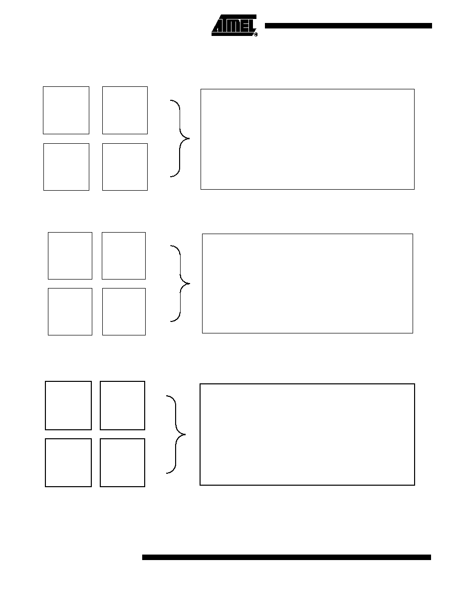
Typical Designs
Figure 1. PC Multimedia
Figure 2. Low-cost Karaoke, Hand-held Karaoke
Figure 3. Low-cost Keyboard Instrument
DAC or
CODEC
CleanWave
ROM
ATSAM9733
SRAM
32K x 8
- General MIDI-compliant Wavetable Synthesis
- MPU401 Interface (UART)
- Compatible Reverb and Chorus
- Surround
- Four-band Parametric Equalizer
- Audio-in Effects (Codec required)
- Serial MIDI-in and -out
- Four-channel Output (extra DAC required)
CODEC
CleanWave
ROM
ATSAM9733
RAM
32K x 16
- General MIDI-compliant Synthesis
- Sound Extensions (CleanWave32)
- Compatible Reverb and Chorus
- MIDI Serial or 8-bit Parallel Interface
- Surround Effect
- Four-channel Surround (requires extra DAC)
- Four-band Equalizer
- Microphone Echo
DAC
CleanWave
ROM
ATSAM9733
RAM
32K x 8
- General MIDI-compliant Synthesis
- Sound Extensions (CleanWave32)
- Compatible Reverb and Chorus
- MIDI Serial or 8-bit Parallel Interface
- Surround Effect
- Four-band Parametric Equalizer
3
ATSAM9733
1714C≠DRMSD≠12/02
General
Description
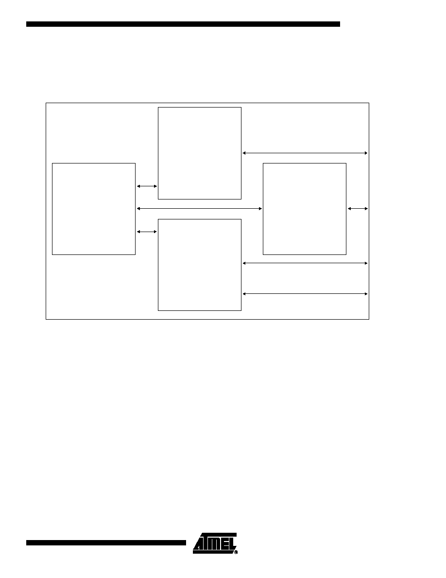
Figure 4. ATSAM9733 Architecture
Synthesis/DSP
Engine
The synthesis/DSP engine operates on a frame-timing basis with the frame subdivided into 64
process slots. Each process is divided into 16 micro-instructions known as algorithms. Up to
32 synthesis/DSP algorithms can be stored on-chip in the Alg RAM memory, allowing the
device to be programmed for a number of audio signal generation/processing applications.
The synthesis/DSP engine is capable of generating 64 simultaneous voices using algorithms
such as wavetable synthesis with interpolation, alternate loop and 24 dB resonant filtering for
each voice. Slots may be linked together (ML RAM) to allow implementation of more complex
synthesis algorithms.
A typical application will use half the capacity of the synthesis/DSP engine for synthesis, thus
providing state-of-the-art 32-voice wavetable polyphony. The remaining processing power will
be used for typical functions such as reverberation, chorus, audio-in processing, surround
effect, equalizer, etc.
Frequently-accessed synthesis/DSP parameter data are stored in five banks of on-chip RAM
memory. Sample data or delay lines that are accessed relatively infrequently are stored in
external ROM or SRAM memory. The combination of localized micro-program memory and
localized parameter data allows micro-instructions to execute in 20 ns (50 MIPS). Separate
buses from each of the on-chip parameter RAM memory banks allow highly-parallel data
movement to increase the effectiveness of each micro-instruction. With this architecture, a sin-
gle micro-instruction can accomplish up to six simultaneous operations (add, multiply, load,
store, etc.), providing a potential throughput of 300 million operations per second (MOPS).
P16 Processor
16-bit CISC Processor
Core Includes
256 x 16 Data RAM
MMU
Memory
Management
Unit
I/O Functions
Includes:
Control/Status
MIDI UART
Timers
Codec Data I/F
Host I/F FIFO
Synthesis/DSP
64 Slots
RISC DSP Core Includes:
512 x 32 Alg RAM
128 x 28 MA1 RAM
256 x 28 MA2 RAM
256 x 28 MB RAM
256 x 16 MX RAM
256 x 12 MY RAM
64 x 13 ML RAM
CODEC +
DAC
ROM
SRAM
MIDI
MPU
PORT

4
ATSAM9733
1714C≠DRMSD≠12/02
P16 Control
Processor and I/O
Functions
The P16 control processor is a general-purpose 16-bit CISC processor core that runs from
external memory. It includes 256 words of local RAM data memory.
The P16 control processor writes to the parameter RAM blocks within the synthesis/DSP core
in order to control the synthesis process. In a typical application, the P16 control processor
parses and interprets incoming commands from the MIDI UART or from the PC ISA interface
and then controls the synthesis/DSP by writing into the parameter RAM banks in the DSP
core. Slowly-changing synthesis functions, such as LFOs, are implemented in the P16 control
processor by periodically updating the DSP parameter RAM variables.
The P16 control processor interfaces with other peripheral devices, such as the system control
and status registers, the on-chip MIDI UART, the on-chip timers and the ISA PC interface
through specialized "intelligent" peripheral I/O logic. This I/O logic automates many of the sys-
tem I/O transfers to minimize the amount of overhead processing required from the P16.
The ISA PC interface is implemented using one address line (A0), a chip-select signal, read
and write strobes from the host, and an 8-bit data bus (D[7:0]).
The data bus can drive the PC bus directly (24 mA buffers). An external plug-and-play IC is
required to map the 16-bit I/O addresses and AEN from the PC onto the address line and chip
select from the ATSAM9733.
The ISA PC interface is normally used to implement a MPU-401 UART-mode-compatible
interface with address 0 being the data register and address 1 being the status/control regis-
ters. Besides the standard two status bits of the MPU-401, two additional bits are provided to
expand the MPU-401 protocol.
Karaoke and keyboard applications can take advantage of the 8-bit MPU-401 interface to
communicate with the ATSAM9733 at high speed with the MIDI-IN and MIDI-OUT signals
remaining available.
Memory
Management Unit
(MMU)
The MMU block allows external ROM and/or RAM memory resources to be shared between
the synthesis/DSP and the P16 control processor. This allows a single device (i.e., SRAM) to
serve as delay lines for the synthesis/DSP and as data memory for the P16 control processor.
5
ATSAM9733
1714C≠DRMSD≠12/02
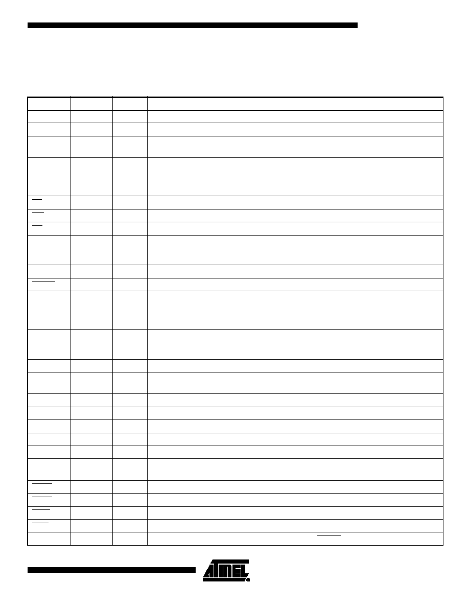
Pin Description
Table 1. Pin by Function
Pin Name
Pin Count
Type
Function
GND
14
PWR
Power Ground. All GND pins should be returned to digital ground.
VC3
4
PWR
Core Power +3.3V ± 10%. All V
C3
pins should be returned to +3.3V.
VCC
11
PWR
Power +3V to +5.5V. All V
CC
pins should be returned to +5V (or 3.3V in case of single 3.3V
supply).
D[7:0]
8
I/O
8-bit data bus to host processor. Has enough driving power to drive ISA PC bus directly (24 mA
buffer).
Information on these pins is parallel MIDI (MPU-401 type applications).
Direct ISA PC bus drive requires 5V V
CC
.
CS
1
IN
Chip select from host, active low.
WR
1
IN
Write from host, active low.
RD
1
IN
Read from host, active low.
A0
1
IN
Selects MPU-401 internal registers.
0: data registers (read/write)
1: status register (read) control register (write)
IRQ
1
TSOUT
Tri-state output pin. Can be connected directly to host IRQ line (24 mA).
RESET
1
IN
Master reset input, active low. Schmitt trigger input.
X1
X2
2
Crystal connection. Crystal frequency should be Fs∑256 (typ 11.2896 MHz).
Crystal frequency is internally multiplied by four to provide the IC master clock.
X1 can also be used as external clock input (3.3V input).
X2 cannot be used to drive external ICs.
DABD[1:0]
2
OUT
Two stereo serial audio data outputs (four audio channels). Each output holds 64 bits
(2 x 32) of serial data per frame. Audio data has up to 20-bit precision, DABD0 can hold
additional control data (mute, A/D gain, D/A gain, etc.).
CLBD
1
OUT
Audio data bit clock, provides timing to DABD[1:0].
WSBD
1
OUT
Audio data word select. The timing of WSBD can be selected to be I2S or Japanese
compatible.
DAAD
1
IN
Stereo serial audio data input.
MIDI_IN
1
IN
TTL level MIDI IN input.
MIDI_OUT
1
OUT
TTL level MIDI OUT output.
WA[20:0]
21
OUT
External memory address (ROM/SRAM). Up to four megabytes of ROM.
WD[15:0]
16
I/O
PCM ROM/SRAM data.
RBS
1
OUT
SRAM byte select. Should be connected to the lower RAM address when an 8-bit wide SRAM
is used. The type of RAM (16-bit/8-bit) can be selected by program.
WCS0
1
OUT
PCM ROM chip select, active low.
WCS1
1
OUT
SRAM chip select, active low.
WWE
1
OUT
SRAM write enable, active low.
WOE
1
OUT
PCM ROM/SRAM output enable, active low.
RUN
1
OUT
High when the synthesis is initialized. Can be used as RESET for an external device (Codec).