 | –≠–ª–µ–∫—Ç—Ä–æ–Ω–Ω—ã–π –∫–æ–º–ø–æ–Ω–µ–Ω—Ç: DES | –°–∫–∞—á–∞—Ç—å:  PDF PDF  ZIP ZIP |
1
Features
∑
Bus-compatible with the ARM7TDMITM Core
∑
16-clock Cycle Encryption/Decryption Process
∑
On Request: 8, 4, 2, 1 Clock Cycle Encryption/Decryption Process
∑
One Key Register
∑
Triple Data Encryption Capability
∑
Fully Scan Testable up to 100%
Description
The Data Encryption Standard (DES) is compliant with the American FIPS (Federal
Information Processing Standard) PUB 46-2 specification. The data and key are
stored in 2 x 32-bit registers. The key register is write-only. An external application is
required to generate the key. Suitable precautions should be taken to protect the secu-
rity of the key.
As soon as data and key are configured, the encryption/decryption process may be
started. 16 clock cycles later, the interrupt is set (if enabled) and the encrypted/
decrypted data is ready to be read out on 2 x 32-bit registers. The DATA_READY sig-
nal indicates that the process is finished and is cleared when the user reads out the
data.
The DES peripheral is compatible with the APB bus of the ARM7TDMI core. It may
also be used with any 32-bit microcontroller.
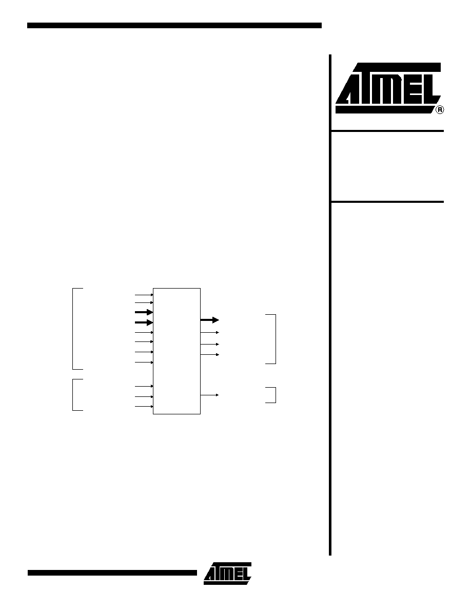
Figure 1. DES Pin Configuration
P_D_IN[31:0]
P_A[13:0]
P_WRITE
P_STB
CLOCK
P_SEL_DES
SCAN_TEST_MODE
IRQ
TEST_SO[2:1]
DES
Functional
Functional
TEST_SE
TEST_SI[2:1]
Scan Test
Scan Test
NRESET
P_D_OUT[31:0]
DES_INT
DATA_READY
P_STB_RISING
32-bit
Embedded Core
Peripheral
Data Encryption
Standard (DES)
Rev. 1351D≠10/01
2
Data Encryption Standard
1351D≠10/01
Note:
One scan chain uses the clock P_STB_RISING while the other uses CLOCK.
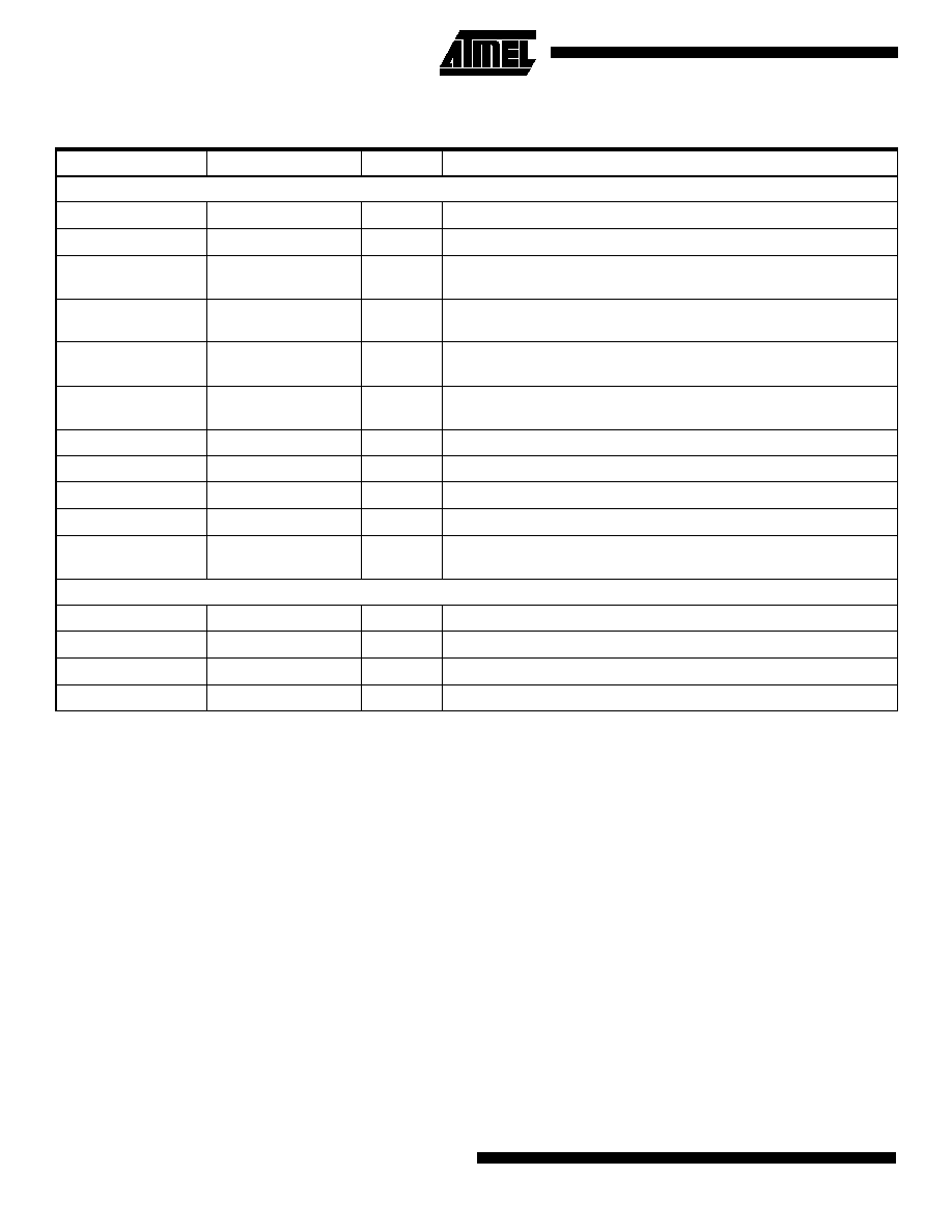
Table 1. DES Pin Description
Name
Function
Direction
Comments
Functional
NRESET
System reset
Input
Asynchronous, active low
CLOCK
System clock
Input
Everything is clocked on this signal except the configuration registers
P_A[13:0]
Software user
interface address bus
Input
The address includes the 2 LSBs [1:0], but the macrocell does not take
into account these bits (left unconnected)
P_D_IN[31:0]
Software user
interface data bus
Input
Data from host (bridge)
P_D_OUT[31:0]
Software user
interface data bus.
Output
Data to host (bridge)
P_WRITE
Transfer enable (from
host to peripheral)
Input
When high, indicates that the host processor is writing to a register or
executing a command
P_SEL_DES
Peripheral selection
Input
Active high
P_STB_RISING
Peripheral strobe
Input
Clock for all DFFs controlling configuration registers
P_STB
Peripheral strobe
Input
When high, indicates that data and address buses are stable
DES_INT
Interrupt
Output
Active high
DATA_READY
Flag
Output
Set when encryption/decryption process is finished
Cleared when data is read out
Scan Test
SCAN_TEST_MODE
Scan test mode
Input
Must be tied high during scan test, must be tied low in functional mode
TEST_SE
Test scan shift enable
Input
Scan shift enabled when tied high
TEST_SI[2:1]
Test scan input
Input
Entry of scan chain
TEST_SO[2:1]
Test scan output
Output
Output of scan chain
3
Data Encryption Standard
1351D≠10/01
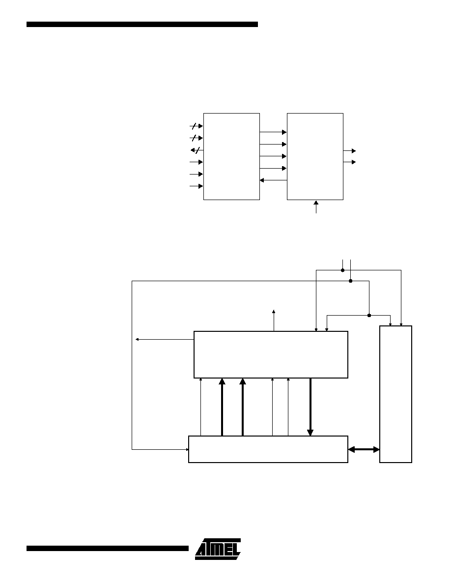
Scan Test
Configuration
The coverage is maximum if all non-scan inputs can be controlled and all non-scan outputs
can be observed. In order to acheive this, the ATPG vectors must be generated on the entire
circuit (top level) which includes the DES or all DES I/Os must have a top level access and
ATPG vectors must be applied to these pins.
Figure 2. DES Timer Block Diagram
Figure 3. Connecting the DES to an ARM
Æ
-based Microcontroller
P_A
P_DIN
P_DOUT
P_WRITE
P_STB
P__STB_RISING
start
ciphering
key
idata
odata
DES_INT
DATA_READY
User
Interface
DES
Algorithm
CLOCK
32-bit
Core
(ARM)
Atmel Bridge
P_WRITE
P_D_IN[31:0
]
P_D_OUT[31:0]
P_STB
P_A[13:0]
P_SEL_DES
Atmel Bus Interface
ASB
DES
To Advanced
Interrupt
Controller (AIC)
DES_INT
NRESET
CLOCK
CLOCK
NRESET
DATA_READY
NRESET
4
Data Encryption Standard
1351D≠10/01
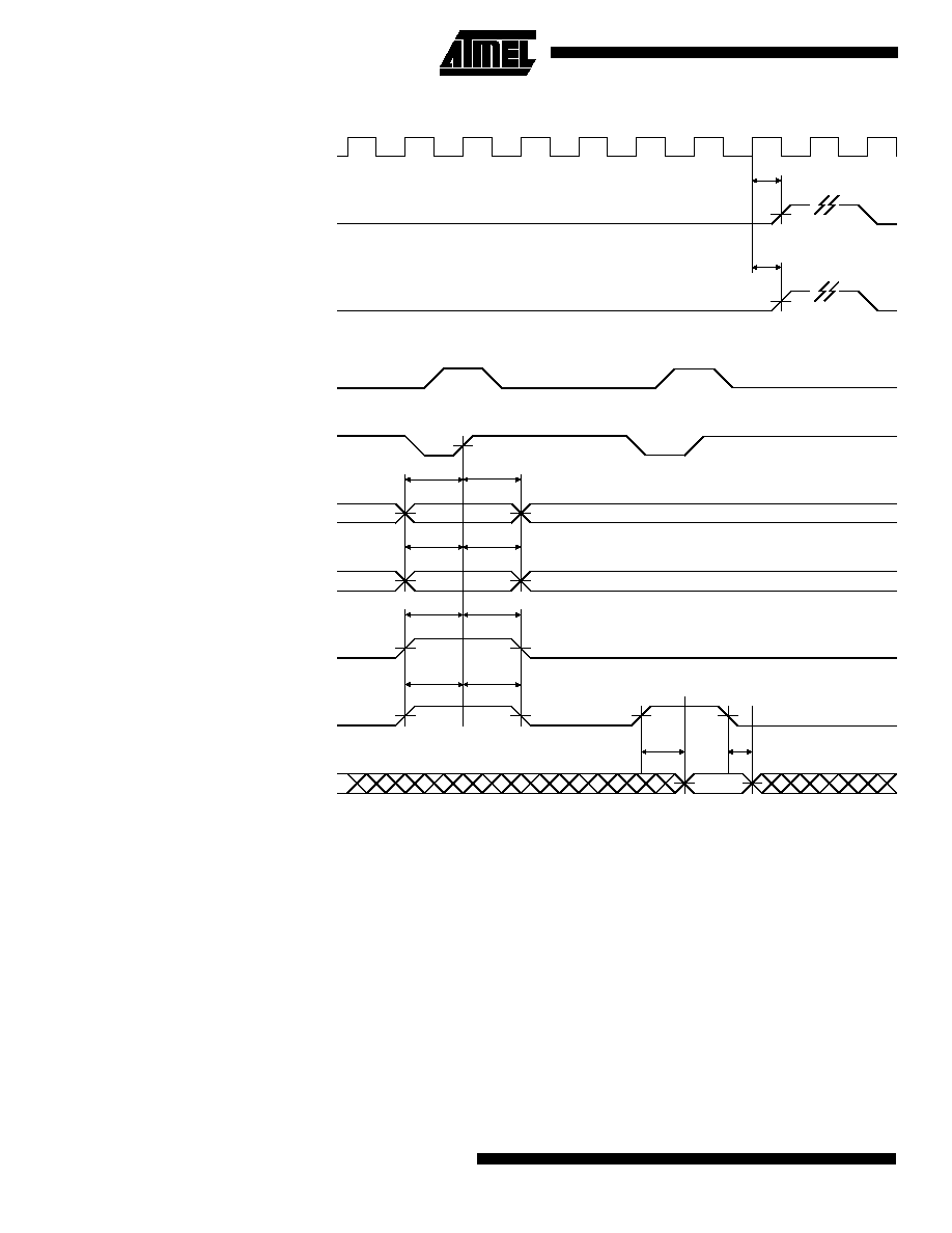
Timing Diagram
Figure 4. DES Timing Diagram
CLOCK
VALID
P_STB
P_A[13:0]
P_D_IN[31:0]
P_WRITE
P_D_OUT[31:0]
t
PD1
t
PD2
t
PD_INT
t
SU_WRITE
t
HOLD_WRITE
t
HOLD_DIN
t
SU_DIN
DES_INT
P_STB_RISING
t
SU_A
t
HOLD_A
t
PD_DATRDY
DATA_READY
P_SEL_DES
t
SU_SEL
t
HOLD_SEL

5
Data Encryption Standard
1351D≠10/01
DES Software User Interface
Notes:
1. The address includes the 2 LSBs [1:0], but the macrocell does not take these bits into account (left unconnected). Therefore,
loading 0x0001, 0x0002 or 0x0003 on P_A[13:0] addresses the Control Register.
2. If the user selects an address which is not defined in the above table, the value of P_D_OUT[31:0] is 0x00000000.
Table 2. DES Memory Map
(1, 2)
Offset
Register
Name
Access Reset
State
0x0000
Control Register
DES_CR
Write-only
≠
0x0004
Mode Register
DES_MR
Read/Write
0
0x0008
Reserved
≠
≠
≠
0x000C
Reserved
≠
≠
≠
0x0010
Interrupt Enable Register
DES_IER
Write-only
≠
0x0014
Interrupt Disable Register
DES_IDR
Write-only
≠
0x0018
Interrupt Mask Register
DES_IMR
Read-only
0
0x001C
Interrupt Status Register
DES_ISR
Read-only
0
0x0020
MSB Key
DES_MKEY
Write-only
0
0x0024
LSB Key
DES_LKEY
Write-only
0
0x0028
Reserved
≠
≠
≠
0x002C
Reserved
≠
≠
≠
0x0030
MSB Input Data
DES_MIDATA
Read/Write
0
0x0034
LSB Input Data
DES_LIDATA
Read/Write
0
0x0038
MSB Output Data
DES_MODATA
Read-only
0
0x003C
LSB Output Data
DES_LODATA
Read-only
0