1
Features
∑
Low-power, Low-voltage CMOS
∑
Rectifier, Voltage Limiter, Clock Extraction On-chip (No Battery)
∑
Small Size
∑
Factory Laser Programmable ROM
∑
Operating Temperature Range -40
∞
C to +125
∞
C
∑
Radio Frequency (RF): 100 kHz to 450 kHz
∑
Transmission options
≠ Code Length: 128, 96, 64, 32 bits
≠ Bitrate [bit/s]: RF/8, RF/16, RF/32, RF/40, RF/50, RF/64, RF/80, RF/100, RF/128
≠ Modulation: FSK, PSK, BIPH, Manchester, BIPH-FSK
∑
FDX-B Compatible Coding Possible (ISO 11784/ ISO 11785)
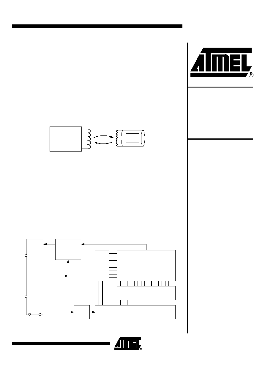
Figure 1. Application
Description
The e5530 is part of a closed coupled identification system. It receives power from an
RF transmitter which is coupled inductively to the IDIC
. The frequency is typically
100 kHz to 450 kHz. Receiving RF, the IDIC
responds with a data stream by
damping the incoming RF via an internal load. This damping-in-turn can be detected
by the interrogator. The identifying data are stored in a 128-bit PROM on the e5530,
realized as an array of laser-programmable fuses. The logic block diagram for the
e5530 is shown in figure 2. The data are output bit-serially as a code of length
128, 96, 64 or 32 bits. The chips are factory-programmed with a unique code.
Figure 2. Block Diagram
RF transmitter
and
interrogator
IDIC
e5530
RF
ID
R7
R6
R5
R4
R3
R2
R1
R0
R
o
w
d
e
c
o
d
e
r
C
1
5
C
1
4
C
1
3
C
1
2
C
1
1
C
1
0
C
9
C
8
C
7
C
6
C
5
C
4
C
3
C
2
C
1
C
0
Column decoder
A
2
A
1
A
0
A
6
A
5
A
4
A
3
Counter
Modulator
FSK
PSK
BIPH
Manchester
Bitrate
Data
Load
Clock
extractor
Rectifier
Mod
Clk
Analog front end
Coil
Coil
V
DD
V
SS
128-bit PROM
128-bit
Read-only
IDIC
for RF
Identification
e5530
Rev. 4508B≠RFID≠02/02
2
e5530
4508B≠RFID≠02/02
Functional Description
Read Operation
After power up, once the e5530 has detected the incoming RF field, the IC continuously
transmits the identification code as long as the RF signal is applied. The transition from
the last bit to bit 1 of the next sequence occurs without interruption. Data is transmitted
by damping the incoming RF signal by an internal load. These load changes are
detected by the reader station.
Different kinds of modulation and bitrates are optionally available.
Rectifier
For internal power supply, an on-chip bridge rectifier is used which consists of two
diodes and two n-channel transistors. A Zener diode, which protects the circuit against
overvoltage on the coil inputs, and a smoothing capacitor for the internal supply are also
provided.
Damping Load
Incoming RF will be damped by the power consumption of the IC itself and by an
internal load, which is controlled by the modulator. The loads are p-channel transistors
connected between V
DD
and the coil inputs.
The IDIC includes mask options for the load circuit: single-side, double-side and
alternate-side modulation.
There are four modulation methods available which can be selected by fuses. The
corresponding timing diagram is shown in Figure 5.
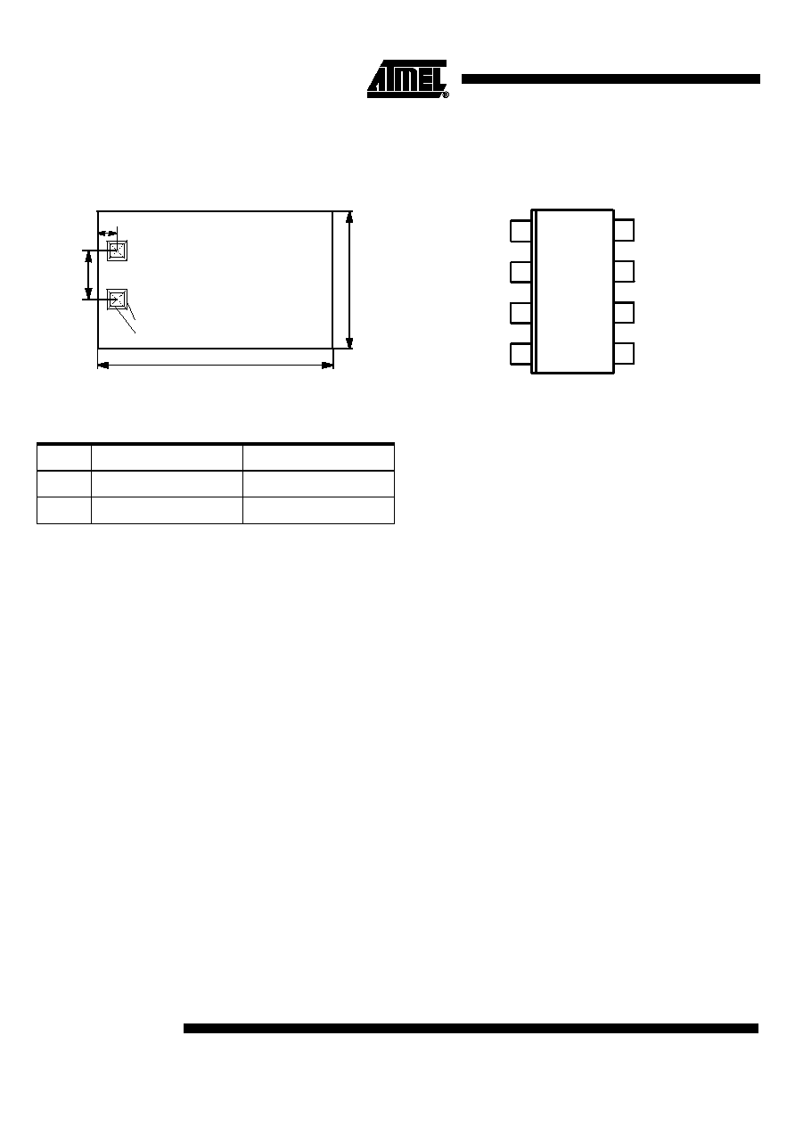
Chip Dimensions
Figure 3. Chip Size
Figure 4. Pinning SO8
Name
Pad Window
Function
Coil1
138
◊
138
µ
m
2
1st coil pad
Coil2
138
◊
138
µ
m
2
2nd coil pad
1
.
1
7
m
m
1.62 mm
Coil 1
Coil 2
0
.
4
4
7
m
m
0.175 mm
Pad: 150
µ
x 150
µ
(Metal: 99% Al, 1% Si
Padwindow: 138
µ
x 138
µ
e5530
Thickness: 15 mils
Coil 1
Coil 2
1
2
3
4
8
7
6
5
Note:
Pins 2 to 7 have to be open. They are
not specified for applications
e5530
3
e5530
4508B≠RFID≠02/02
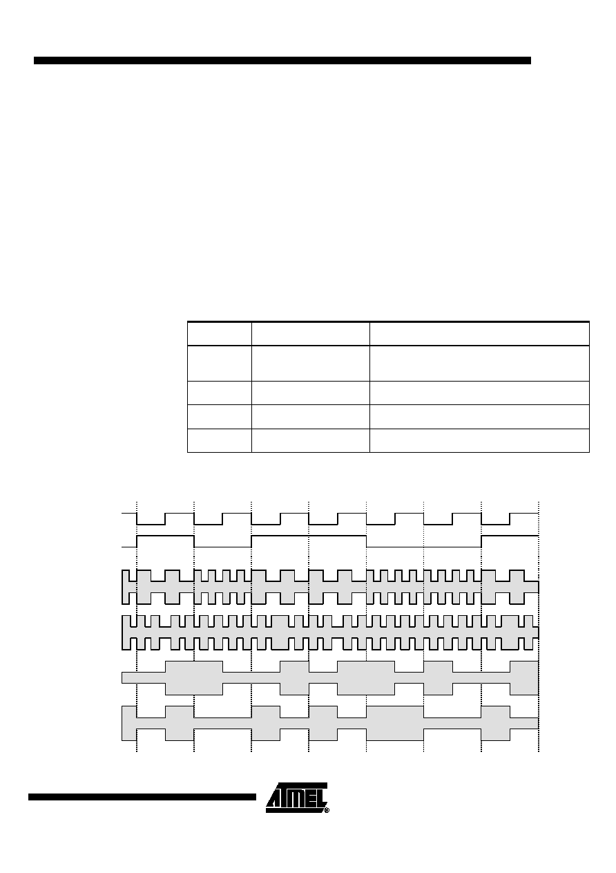
FSK Modulation
Logical data "1" and "0" are represented as two different frequencies of damping. The
frequency for "1" is RF divided by 10, a "0" divides RF by 8.
PSK Modulation
The external coil is damped with a carrier frequency of RF/2. A logical "1" causes (at the
end of the bit period) a 180
∞
phase shift on the carrier frequency, while a logical "0"
causes no phase shift.
Biphase Modulation
Logical "1" produces a signal which is the same as the internal bitclock. A logical "0"
produces no signal change in the middle of the bit period.
Manchester Modulation
A logical "1" causes a rising edge in the middle of a bit period (i.e., switch damping off),
while a logical "0" causes a falling edge (i.e., switch damping on).
A combination of Biphase- and FSK-modulation is also optionally available. The
available combinations between the modulation types and the bitrates are shown in
Table 1 "Transmission Options".
Table 1. Transmission Options
Figure 5. Timing Diagram for Modulation Options
Modulation
Carrier Frequency (CF)
Bitrate [bit/s]
FSK
RF/8, RF/10
RF/32, RF/40, RF/50, RF/64, RF/80, RF/100,
RF/128
PSK
RF/2
CF/4, 8, 16, 32
Biphase
RF/8, RF/16, RF/32, RF/64, RF/100, RF/128
Manchester
RF/8, RF/16, RF/32, RF/64, RF/100, RF/128
BitClk
Data
PSK
FSK
Biph
Man
1
1
1
1
0
0
0
4
e5530
4508B≠RFID≠02/02
Reading Distances
The e5530 is able to operate from very weak fields. Nevertheless, there are some
general rules which influence the achievable reading distance.
∑
Best results are accomplished when the transponder points towards the reader coil.
∑
The transponder should not be embedded in metal, which will reduce the applicable
magnetic field and thus the reading distance.
∑
The strength of the generated magnetic field and the sensitivity of the demodulator
are the most important factors for a good reading distance.
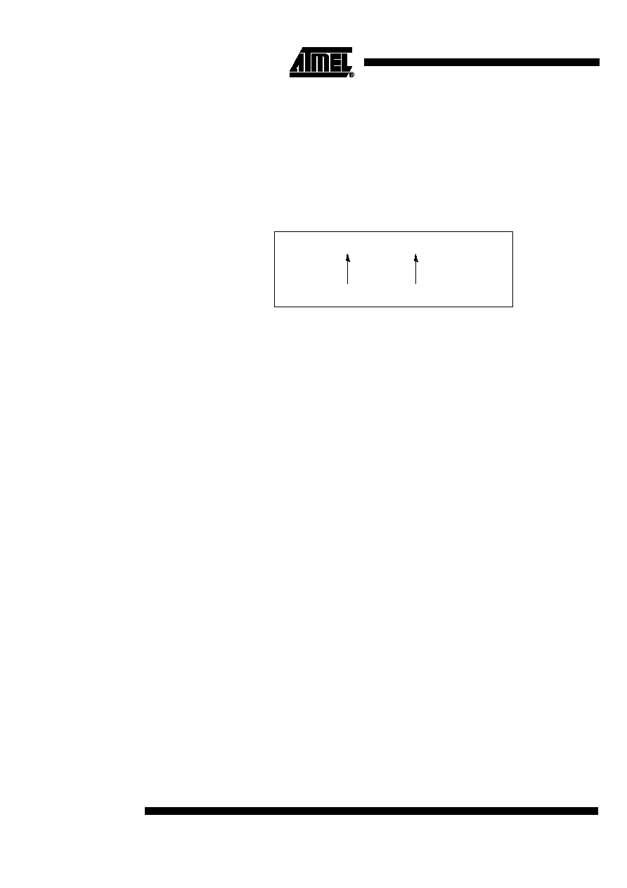
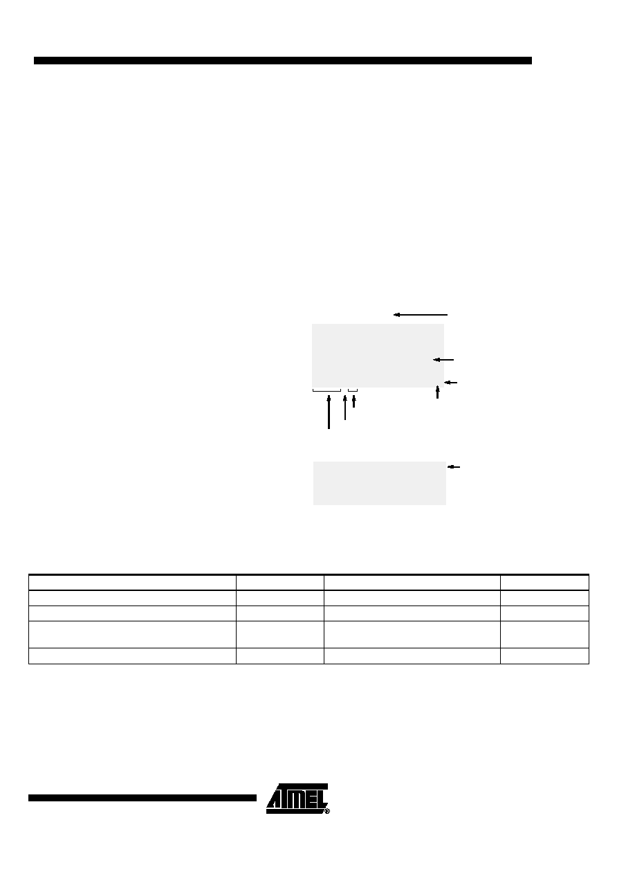
Figure 6. Example for a 64-bit Code
The identification code is transmitted continously. After the RF field is applied, the
e5530H-232 starts with the first bit (MSB) of the header byte 'E6hex' ('1110 0110'),
followed by a unique 56-bit serial number. No checksum is included in this sample code.
Pulsing the RF field may reduce the synchronization task as the first byte transmitted is
known already (i.e., E6hex). This is even feasible, if the first bit may be lost due to
reader synchronization problems.
Customer ID Code
Selection
In general the customer may choose any ID code suitable to his application. To avoid
code duplication, Atmel will define a fixed header
≠
i.e, the first 8 bits of the code
≠
for
each customer.
Modes of Operation ≠
Options
For any new product variant, the customer has to select the following operation options
which are configured in the laser ROM as well:
∑
Bitrate, which is defined as field clocks per bit (e.g., RF/40 = 125 kHz/40 =
3.125 kBit/s) (see table Table 1 "Transmission Options")
∑
Modulation method (see Figure 5)
∑
Code length: 32, 64, 96 or 128 bits
For programming the ID code into the laser ROM, one of the following data has to be
supplied:
∑
ID code algorithm which is implemented in Atmel's code management software
(Atmel will generate the codes as requested)
∑
Customer generated ID codes on floppy disk or per email/ftp.
The format has to comply to the following rules:
≠
The ID code file is a plain ASCII text file.
≠
The code files should be compressed. Please make self extracting files.
≠
The code files are used in alphabetical order of their file names (including
letters and numbers). Used - i.e. programmed - code files are discarded.
≠
Each line of the code file must contain one ID code for one IC.
≠
The code is in hexadecimal format. The code may contain spaces for better
readability.
E6
Header
56-bit ID code
00 00 00 10 2D 72 5D
5
e5530
4508B≠RFID≠02/02
≠
The code line is exactly as long as the selected code length (e.g. 64 bits 16
hex numbers).
≠
The line must end with a carriage return.
≠
The first 8 bits are fixed, this is the unique customer header which is defined
by Atmel.
≠
Each hexadecimal code entry must be preceded by a decimal serial number.
Serial number and code must be separated by a space.
≠
The serial number has to be unique and is up-counting to avoid double
programming.
≠
The series numbers of two consecutive files (file name!) has to count also
for proper linking.
Figure 7. Example of Two Code Files with Header = E6 and 64-bit Code Length
00001 E65F34E25801904F
00002 E634E25801904FAA
00003 E6910AG7000010FE
...
...
12345 E610ABE4F9014821
12346 E6A04EB73087FCC0
12347 E60178DC00F03460
...
FILE0000.TXT
FILE0001.TXT
File name
Series number
Space necessary
Carriage return
Last code
Next
code
8-bit header
Code file
Absolute Maximum Ratings
Parameters
Symbol
Value
Unit
Maximum current into Coil1 and Coil2
I
coil
10
mA
Maximum power dissipation (dice)
P
tot
100
mW
(1)
Maximum ambient air temperature with voltage
applied
T
amb
-40 to +125
∞
C
Storage temperature
T
stg
-65 to +200
∞
C
Note:
1. Free-air condition. Time of application: 1 s
Stresses above those listed under `Absolute Maximum Ratings' may cause permanent damage to the device.
Functional operation of the device at these conditions is not implied.