1
Features
∑
Four Independent Receivers
∑
OneTransmitter in A Mode
∑
Direct 6800 Microprocessor Interface
∑
8-bit Data Bus
∑
ARINC Interface: "1" and "0" Lines, RZ Code
∑
Software Label Control in A Mode
∑
Parity Control: Odd or No Parity
∑
Interrupt Capability in A Mode
∑
Test Mode Capability
Description
The EF4442 is a reception interface for 4 ARINC 429 channels.
Two models of operation are provided:
∑
When in A mode, the circuit can be considered as a peripheral of an EF 6800 or
EF6802 microprocessor and is totally software programmable (for example, for
test purposes).
∑
When in B mode, the parameters are hardware programmed. Reading the
registers which contain messages is only possible (max. scan frequency: 2 MHz).
Screening Quality
This product is manufactured in full compliance with either:
∑
NFC 96883 class G
∑
MIL-STD-883 class B
∑
According to Atmel standards
Application Note
Ask for application note: "General application principles EF4442(RTA)"
C Suffix
DIL 28
Ceramic Side Brazed package
P Suffix
DIP 28
Plastic Package
ARINC 429
Multi-channel
Buffer Receiver
(RTA)
(N Channel,
Silicon Gate)
EF4442
Rev. 2112A≠HIREL≠11/02
2
EF4442
2112A≠HIREL≠11/02
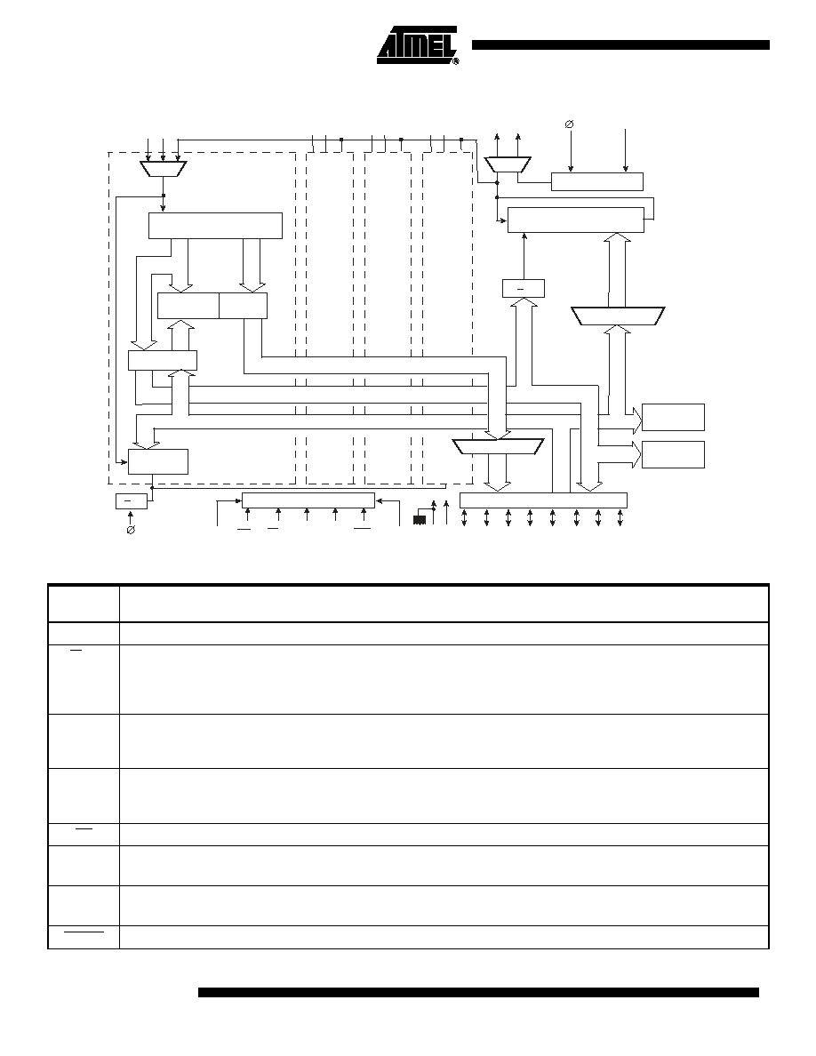
Figure 1. Block Diagram
Shift register
32 bits
Comparator
8 bits
Buffer
24 bits
HR
8
24
24
8
8
8
8
8
Synchro
enable
Control
Buffer
MODE CS
A0
D0 D1 D2 D3 D4
D5 D6 D7
A1
RW/INH
IRQ/V
VSS VCC
: 8
Status
Control
register
Shift register
32 bits
DEMUX 1 -> 3
32
HE
8
8
8
6
8
8
8
: n
Counter N0, N1
H1 L1
H0 L0
H2 L2
H3 L3
N0 N1
INH
Channel 0
Channel 1
Channel 2
Channel 3
Label
MUX 3 -> 1
24
Table 1. Pin Description
Name
Number
Description
V
SS
This pin is connected to the negative side of the power supply (ground).
RW/INH
This input selects the direction of transfer (write or read) of data between the circuit and the microprocessor when the
circuit is programmed in mode A (cf. Pin 28).
In B mode, this input is used to disable the channel scanning divide by 4 counter. In A mode, this output has a transmit
function. The signal corresponding to the result of ANDing.
N0
In A mode, this output has a transmit function. The signal corresponding to the result of ANDing the ARINC transmit
clock and the complemented output signal of the transmit shift register (logic "0" clock output) is available on this pin.
In B mode, the value of the least significant bit of the address of the scanned channel is available on this pin.
N1
In A mode, this output has a transmit function. The signal corresponding to the result of ANDing the ARINC transmit
clock and the output signal of the transmit shift register (logic "1" clock available on this pin).
In B mode, the value of the least significant bit of the address of the scanned channel is available on this pin.
CS
In A mode, this input (active when low) selects the chip for a microprocessor access.
A0
In A mode, this input corresponds to the most significant bit of the circuit function address.
In B mode, this input corresponds to the least significant bit of the address of the data byte in the message.
A1
In A mode, this input corresponds to the most significant bit of the circuit function address.
In B mode, this input corresponds to the most significant bit of the address of the data byte in the message.
RESET
This input (active when low) initializes the circuit by resetting some registers.

3
EF4442
2112A≠HIREL≠11/02
Description of
Registers
The EF4442 circuit features three types of internal register:
∑
Registers concerned with general circuit operation,
∑
Registers specific to the transmit channel,
∑
Registers specific to each receive channel.
General Registers
Status Register
This register is used only when the circuit is programmed in A mode. Its contents inform
the microprocessor about the status of the circuit functions. Bits S0 and S4 activate out-
put IRQ when at 1 (except S4 which is maskable - cf. description of control register).
Bits S0 and S3 at 1 indicate that the channel with the address which corresponds to the
rank of the bit has received a correct message (label recognized and correct parity in the
case of a circuit programmed to check the parity of messages).
Each bit is reset to 0 on reading the registers of the corresponding channel.
In transmit mode, bit S4 of the status register is set to 1 when transmission of the mes-
sage is terminated.
ÿ
This input receives the clock signal from the circuit which corresponds to the phase ÿ2 of the microprocessor clock.
D7
This tristate input/output is connected to the eighth line of the data bus.
D6
This tristate input/output is connected to the seventh line of the data bus.
D5
This tristate input/output is connected to the sixth line of the data bus.
D4
This tristate input/output is connected to the fifth line of the data bus.
V
CC
This pin is connected to the positive side of the power supply (+5V).
D3
This tristate input/output is connected to the fourth line of the data bus.
D2
This tristate input/output is connected to the third line of the data bus.
D1
This tristate input/output is connected to the second line of the data bus.
D0
This tristate input/output is connected to the first line of the data bus.
L0
This input receives the logic "0" clock from the signal shaping/separation subsystem of the first ARINC channel.
H0
This input receives the logic "1" clock from the signal shaping/separation subsystem of the first ARINC channel.
L1
This input receives the logic "0" clock from the signal shaping/separation subsystem of the second ARINC channel.
H1
This input receives the logic "1" clock from the signal shaping/separation subsystem of the second ARINC channel.
L2
This input receives the logic "0" clock from the signal shaping/separation subsystem of the third ARINC channel.
H2
This input receives the logic "1" clock from the signal shaping/separation subsystem of the third ARINC channel.
L3
This input receives the logic "0" clock from the signal shaping/separation subsystem of the fourth ARINC channel.
H3
This input receives the logic "1" clock from the signal shaping/separation subsystem of the fourth ARINC channel.
IRQ/V
In A mode, this pin (active when low) constitutes an open drain output delivering the signal for interrupting the
microprocessor.
In B mode, this pin is an input used to program the number of high speed channels.
Mode
This input is used to program the operating mode (A or B) of the circuit and also to enable or disable this parity check.
Table 1. Pin Description (Continued)
Name
Number
Description

4
EF4442
2112A≠HIREL≠11/02
Bit S4 is reset to 0 when control bit C4 (see below) is a 1.
Bits S5 and S6 are not used.
Bit S7 is at 1 throughout transmission.
Control Register
This eight-bit register (C0-C7) monitors operation of the circuit in A mode.
In receive mode, bits C0-C3 select the corresponding channels for writing or reading
when set to 1 by the microprocessor.
Bit C4 at 1 enables programming of the transmit channel (data to send and transmission
speed). The setting of bit C4 to 1 resets to 0 the index of the four-byte stack constituting
the message to send.
Bit C5 at 1 is used to initiate transmission of the message. It is set to 0 when transmis-
sion is terminated.
Bit C6 at 1 simultaneously with bit C5 at 1 loops back the transmitted data to the input of
the receive channel selected by bits C0-C3, for test purposes. It is set to 0 by any control
register access.
Bit C7 at 1 masks status bit S4 and thus prevents activation of output IRQ.
Transmit Channel
Registers (A mode only)
Programmable Divider
Register
This eight-bit register is programmed by the microprocessor and contains the value n of
the division ratio (the least significant bit is always considered to be at 0).
The programmable divider generates a clock signal at a frequency equal to clock ÿ
divided by n.
Transmit Register
This 32-bit shift register may be programmed in four phases by the microprocessor. This
writing must be effected immediately after the setting to 1 of control bit C4 (cf. descrip-
tion of control register). This resets to zero the index of the 4-byte stack.
The transmit register shifts the data present in it to the outputs in accordance with the
states of the bits in the control register.
Receive Channel
Registers
Each receive channel comprises the following registers:
Synchronization/Enable
Register
This eight-bit register is programmable by the microprocessor.
The most significant bit (bit 7) is used, in A mode only, to disable the transfer of data at
the input into the buffer register (cf. description of these two registers). The channel
affected is then seen as being out of service.
The other seven bits (bits 0 - 6) select the value of the time-delay used to detect the
presence of a "gap". This is the space between two consecutive messages, the mini-
mum duration of which is four periods of the transmit clock. This value is loaded into the
register by the microprocessor, in A mode, at the same time as the enable bit.
In B mode, this value is selected from two hardwired values, according to the state on
pin IRQ/V.
If n is the programmed value, the gap detection time-delay will be (8n - 4) ± 4 period of
clock ÿ.
5
EF4442
2112A≠HIREL≠11/02
Input Register
This 32-bit shift register receives the data corresponding to the messages. The mes-
sage received is transferred into the registers on its output side if:
∑
a gap detection signal has previously occurred,
∑
the registers which will receive the transferred data are not being read,
∑
the parity of the received message is correct if the circuit is programmed with the
parity check enabled,
∑
the enable bit of the synchronization/enable register is set to 1 (A mode only),
∑
in A mode, the first eight bits received correspond to the programmed label (cf.
description of label register).
Label Register
In A mode, this eight-bit register is programmed by the microprocessor. It contains the
label to be recognized.
In B mode, this register receives the first eight bits of the received message transferred
from the input register.
In this case, this register may be read by the external automatic scanning device.
Buffer Register
This 24-bit register receives data transferred from the input register.
It may be read by the microprocessor in A mode or by the external automatic scanning
device in B mode.
Circuit Operation
Logic Convention
"1" (high state) = most positive level
"0" (low state) = most negative level
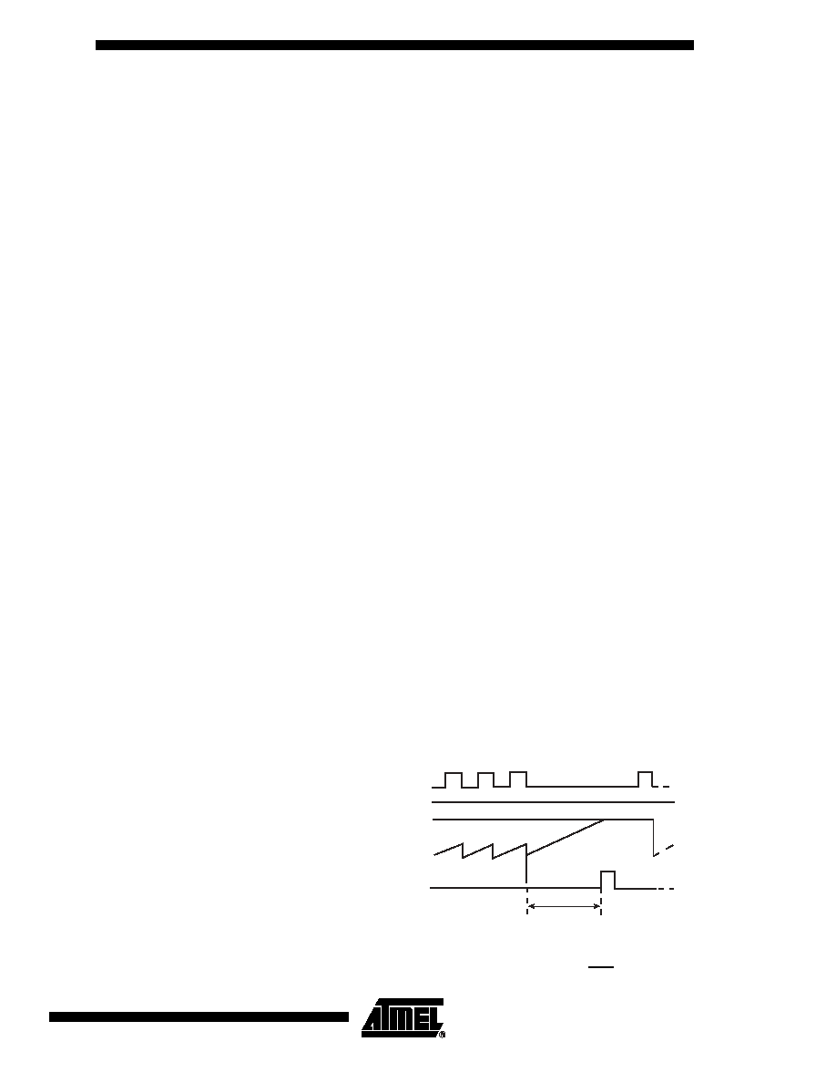
Operation of a Receive
Channel
Data Acquisition
Serial data is received on the "low" and the "high" lines (Hi and Li inputs). The Clock is
reconstructed by OR-ing these inputs. Data is then directed towards a 32-bit shift regis-
ter. Parity is computed. The reconstructed clock fall edge resets the message
synchronization counter. This counter is incremented on each ÿ: 8 clock period and
delivers a word synchronization signal (gap) as described below (Figure 2) when read-
ing a programmed value.
Figure 2. Gap Detection
The predetermined value together with an enable bit is loaded in the internal syn-
chro/validation register when in A mode; it is chosen between two hardware
programmed values when in B mode, according to the IRQ/V pin.
Clock
max
gap
Counter
0
Synchro
Predetermined value