1
Features
∑
Low Drop Out Voltage Regulator
∑
4.5V Fixed Output Voltage
∑
4.75V to 5.5V Supply Operation
∑
30 mA Maximum Load Current
∑
Less Than 162 µA (max) Quiescent Current
∑
Power-down Mode Consumption Less Than 1 µA
∑
More Than 50 dB (Typical) PSRR at 1 kHz
∑
60 µV
RMS
Output Noise
∑
0.35 µm CMOS Technology
∑
Typical Application: Radio Frequency Synthesizer and Antenna Switch Controller
Section Supply in Mobile Terminals
Description
RE028 is a Low Drop Out (LDO) voltage regulator macrocell with a fixed 4.5V output
voltage, rated for loads up to 30 mA. It is designed to be integrated with other analog
cells, digital logic, microcontrollers, DSP cores and memory blocks into system-on-
chip products. Furthermore, the RE028 is designed to supply radio frequency synthe-
sizers and used as a controller for the antenna switch.
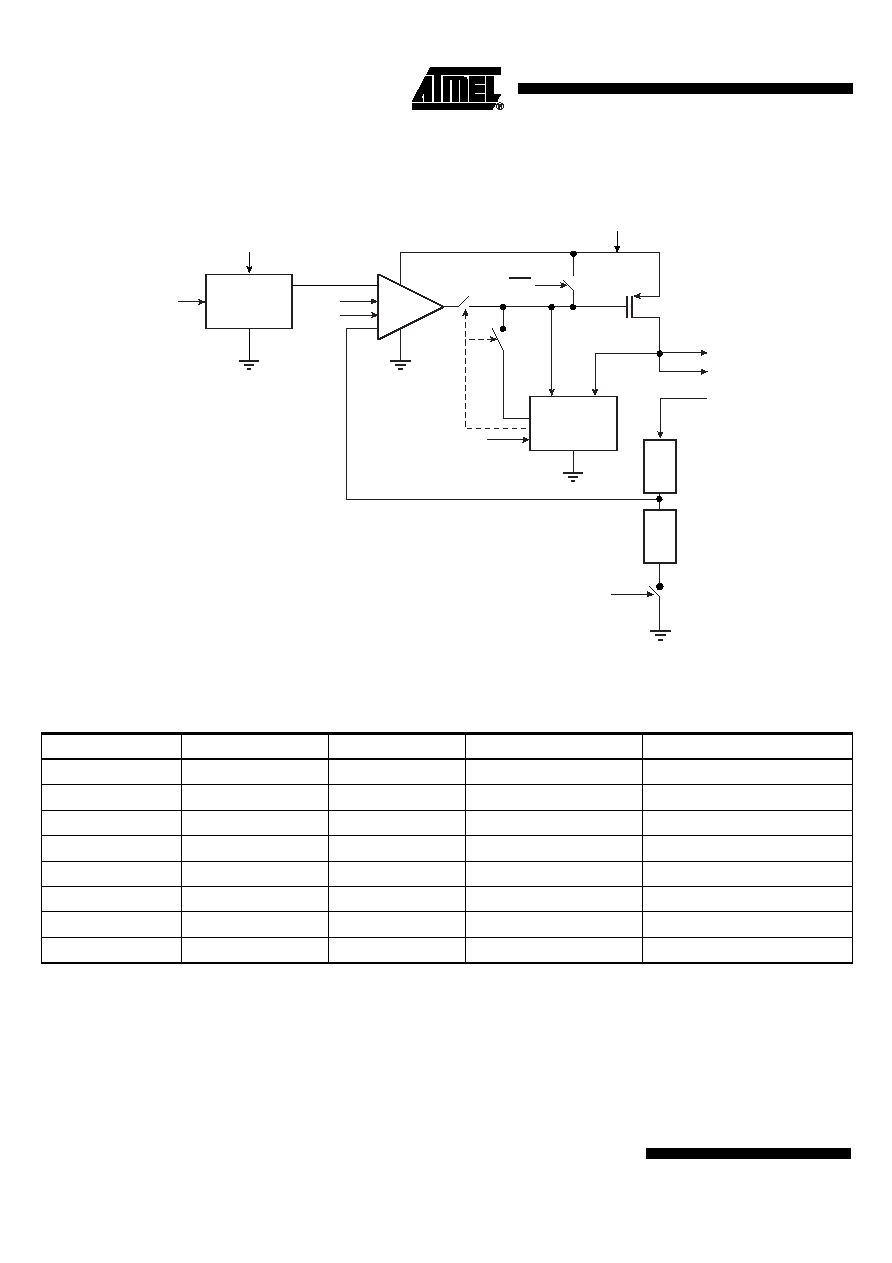
The circuit consists of a PMOS pass device, an error amplifier and a feedback resis-
tive network, sized to achieve the required closed loop gain. These blocks make up
the regulating loop. An over-current and short circuit protection circuit has been
included to limit the output current delivered by the regulator, thus avoiding destruction
in case of a short circuit.
An external reference voltage (bandgap voltage) is necessary for correct functionality.
The target reference voltage is 1.231V, delivered, for example, by BG019. Current ref-
erence is generated inside the cell through a circuit supplied by a 2.5V ± 0.1V
regulated input voltage on V
SAUVC
. Remote sense terminal V
RADS
provides regulation
at the load by connecting it to the output terminal near a critical point to improve per-
formance of the regulator (e.g., connecting them at the package pin by double-
bonding, thus avoiding the bonding resistance influence). A ceramic capacitor of 2.2
µF connected from V
RAD
to ground is needed as external compensation.
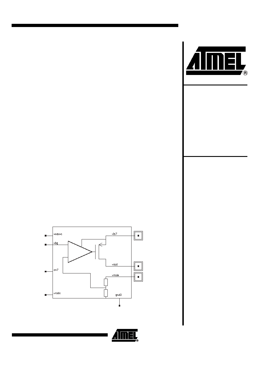
Figure 1. Symbol
(1)
Note:
1. Pin names are written as they appear on the user screen when the symbol is
opened in the design tool environment.
Embedded ASIC
Macrocell:
Power
Management for
Mobile
Terminals (PM)
RE028
Fixed 4.5V
30 mA
LDO Voltage
Regulator
Rev. 2704B≠PMGMT≠03/03
3
RE028 4.5V 30mA LDO Voltage Regulator
2704B≠PMGMT≠03/03
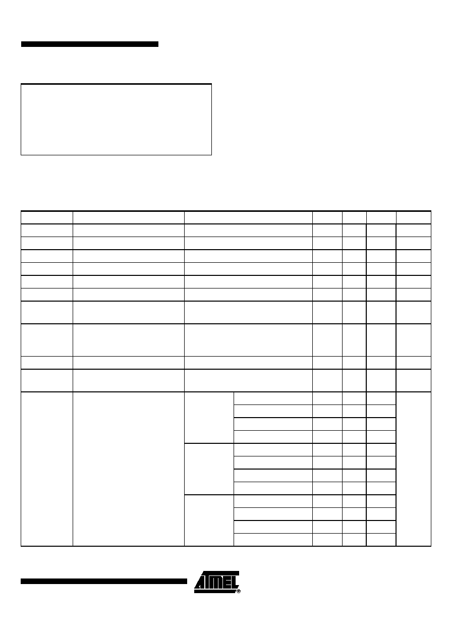
Absolute Maximum Ratings
*
Electrical Specifications
(1)
T
J
= -20
∞
C to 125
∞
C, V
IN7
= 4.75V to 5.5V unless otherwise specified, output capacitance = 2.2 µF.
V
IN
.......................................................... -0.3V to 6.5V
*NOTICE:
Stresses beyond those listed under "Absolute Maxi-
mum Ratings" may cause permanent damage to the
device. This is a stress rating only and functional
operation of the device at these or other conditions
beyond those indicated in the operational sections of
this specification is not implied. Exposure to absolute
maximum rating conditions for extended periods may
affect device reliability.
Digital Signals......................................... -0.3V to 5.5V
Output Current..................................Internally Limited
Junction Temperature ..........................-40
∞
C to 150
∞
C
Table 1. Electrical Specifications
Symbol
Parameter
Condition
Min
Typ
Max
Unit
V
IN7
Operating supply voltage
4.75
5.1
5.5
V
V
SAUVC
Auxiliary operating supply voltage
2.4
2.5
2.6
V
T
J
Junction temperature range
-20
125
∞C
V
RAD
Output voltage
4.4
4.5
4.6
V
I
RAD
Output current
30
mA
I
QQ
Quiescent current
138
162
µ
A
V
DC
Line regulation
V
IN7
from 4.75V to 5.5V,
I
RAD
= 30 mA
3
mV
V
TRAN
Transient line regulation
V
IN7
from 4.75V to 5.5V,
I
RAD
= 30 mA,
rise time = fall time = 5
µ
s
35
mV
V
DC
Load regulation
10% to 90% of max I
RAD
3
mV
V
TRAN
Transient load regulation
10% to 90% of max I
RAD
,
rise time = fall time = 5
µ
s
17
mV
PSRR
Power supply rejection ratio
V
IN7
= 4.75V
@ 100 Hz
-60
dB
@ 1 kHz
-50
@ 20 kHz
-20
@ 100 kHz
-20
V
IN7
= 5.1V
@ 100 Hz
-70
@ 1 kHz
-65
@ 20 kHz
-45
@ 100 kHz
-35
V
IN7
= 5.5V
@ 100 Hz
-65
@ 1 kHz
-60
@ 20 kHz
-50
@ 100 kHz
-40
4
RE028 4.5V 30mA LDO Voltage Regulator
2704B≠PMGMT≠03/03
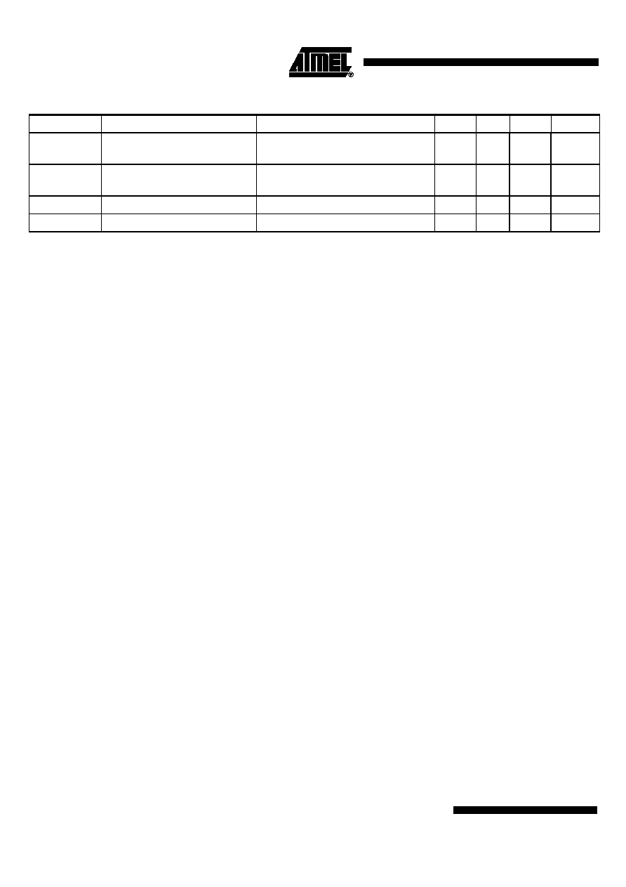
Notes:
1. Obtained by considering the parasitics of a TFBGA100 Package.
2. Obtained by using BG019 as reference voltage generator.
V
N
Output noise
(2)
Bandwidth: 10 Hz to 100 kHz
I
RAD
= 30 mA
60
80
µ
Vrms
T
R
Rise time
100% of I
RAD
,
10% to 90% of V
RAD
230
300
µ
s
I
SD
Shut down current
1
µ
A
I
CC
Short-circuit current
82
100
mA
Table 1. Electrical Specifications (Continued)
Symbol
Parameter
Condition
Min
Typ
Max
Unit
5
RE028 4.5V 30mA LDO Voltage Regulator
2704B≠PMGMT≠03/03
Control Modes
All digital signals are referred to the supply voltage V
IN7
.
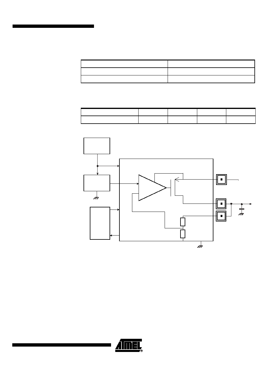
Application Example
A ceramic capacitor of 2.2 µF with ESR between 20 m
and 250 m
connected from
V
RAD
to ground is needed as external compensation.
Figure 3. Application Example
Table 2. Truth Table
ON7
V
RAD
0
Power down (High-Z)
1
Power on, V
RAD
= 4.5V
Description
Min
Typ
Max
Units
Capacitor, C
L
1.8
2.2
2.6
µF
Digital
Core
1.231V Bandgap
(e.g., BG019)
2.5V
2.5V Regulator
(e.g., RE031)
V
IN7
V
RAD
V
RADS
V
SAUVC
V
BG
ON7
V
RADC
GND3
C
L
Input
Supply