 | –≠–ª–µ–∫—Ç—Ä–æ–Ω–Ω—ã–π –∫–æ–º–ø–æ–Ω–µ–Ω—Ç: STSAM9708 | –°–∫–∞—á–∞—Ç—å:  PDF PDF  ZIP ZIP |
1772D≠DRMSD≠01/04
Features
∑
Up to 128-voice Top-quality Wavetable Synthesis Chip
≠ Two 64-voice RISC DSP Cores
≠ Two High-speed CISC Control Processors
≠ Versatile Programmable Digital Audio Routing Between the Two DSPs
∑
Voices Can Be Allocated for Synthesis and/or Effects and/or Audio Processing
∑
Maximum Single-shot PCM Wavesize of 4M Samples (93 Seconds @ 44.1 kHz)
∑
Samples Can Be Stored in 16-bit Floating Point Format (20-bit Dynamic), 16-bit Linear,
8-bit Linear
∑
Standard Audio Processing Firmware Includes Equalizer, Surround, MPEG Audio
Decoder (Level 2)
∑
Sophisticated Built-in Cache Memories
≠ Allows Use of Standard 90 ns 16-bit ROMs/RAMs
≠ Guarantees Crisp Response Even Under Heavy Traffic Conditions
∑
GS
Æ
Sound Set
(1)
under License from Roland
Æ
Corporation, Other Sound Sets
Available
∑
16-channel Audio-in, 16-channel Audio-out @ 22 Bits Audio/Channel
∑
28-bit Internal Audio Path
∑
Two Serial MIDI-In, Two Serial MIDI-Out
∑
Firmware/Wavetable Data Can Reside in ROM, DRAM, SDRAM
∑
Up to 256M Bytes of External Memory with Support of SIMM (DRAM) and DIMM
(SDRAM)
∑
High-speed 16-bit Burst Transfer for Firmware Download or Streaming Audio
∑
Compatible with ATSAM9707, Uses Proven Design and Development Tools
≠ Sound Editor, Sound Bank Editor
≠ Algorithm Compiler, Assembler, Source Debugger
≠ Direct Development from PC Environment, No Special Emulator Required
∑
Top Technology
≠ Single Low-frequency Crystal and Built-in PLL
≠ 3.3V Supply, 5V-tolerant I/Os
≠ Space-saving 144-lead TQFP Package
≠ Power-down Mode
∑
Typical Applications: Karaokes, High-range Multimedia, Classical Organs, Digital
Pianos, Professional Keyboards, Musical Samplers
Note:
1. The GS Sound Set is subject to special licensing conditions. Not to be used for
musical instruments.
Description
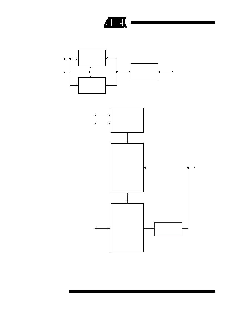
The ATSAM9708 is a 128-voice integrated synthesizer, integrating two PDSP blocks
and a memory management unit (MMU). One PDSP block is a combination of a spe-
cialized 64-slot RISC-based digital signal processor (DSP), a general-purpose 16-bit
CISC-based control processor (P16), a cache memory and an "intelligent" peripheral
I/O interface. Both PDSPs are fully independent and share the same external memory
through the MMU.
Sound
Synthesis
ATSAM9708
128-voice
Integrated
Sound
Synthesizer
2
ATSAM9708
1772D≠DRMSD≠01/04
Block Diagrams
Figure 1. ATSAM9708 Block Diagram
Figure 2. PDSP Block Diagram
PDSP 1
PDSP 2
MMU
Memory
MIDI and Audio
16-bit Bus
16-bit Bus
MIDI
Audio
MMU
I/O Functions
Control/Status
MIDI UART
Timers
Host I/F
P16 Processor
16-bit CISC
Processor Core
Includes
256 x 16 Data RAM
256 x 16 Boot ROM
Synthesis/DSP
RISC DSP Core
Includes
512 x 38 Alg RAM
128 x 28 MA1 RAM
256 x 32 MA2 RAM
256 x 32 MB RAM
128 x 16 MX RAM
256 x 16 MY RAM
64 x 13 ML RAM
Cache Memory
128 x 16
3
ATSAM9708
1772D≠DRMSD≠01/04
Pin Description by Function
Notes:
1. ISA bus group pins are powered by V
CC1
power rail.
2. PC_D pads have 4 mA drive capabilities; other output pads have 16 mA drive capabilities.
3. To interface with PC ISA bus, V
CC1
should be connected to 5V power and PC_D bus should be buffered. Direction is given by
PC_RD signal.
4. Pin Names in this document exhibiting an overbar (PC_CS for example) indicates that the signal is active low.
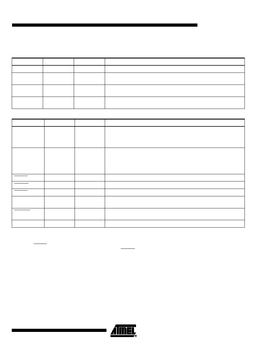
Table 1. Power Group
Name
Pin Count
Type
Function
GND
19
PWR
Power Ground. All GND pins should be returned to digital ground.
VC3
8
PWR
Core Power, +3.3V nominal (3V to 4.5V). All V
C3
pins should be returned to
+3.3V.
VCC1
5
PWR
Pad (except Memory Pad) Power, +3.0V to +5.5V. All V
CC
pins should be
returned to +5V (or 3.3V in case of single 3.3V supply).
VCC2
5
PWR
Memory Pad Power, +3.0V to +5.5V. All V
CC
pins should be returned to +5V (for
RAM or DRAM) or 3.3V (for SDRAM or 3.3V ROM).
Table 2. ISA Bus Group
(1)
Name
Pin Count
Type
Function
PC_D[15:0]
(2, 3)
16
I/O
16-bit data bus to host processor.
Information on these pins is:
- 2 x parallel MIDI (MPU-401 type applications)
- 2 x high-speed burst data transfers to/from external memory
PC_A[2:0]
3
IN
Selects one of 8 internal registers:
0, 1: MPU-401 register processor #1
2, 3: Burst data (16-bit) processor #1
4 - 5: MPU-401 register processor #2
6 - 7: Burst data (16-bit) processor #2
PC_CS
(4)
1
IN
Chip select from host, active low.
PC_WR
1
IN
Write from host, active low.
PC_RD
1
IN
Read from host, active low.
PC_READY
1
TSout
Open drain output buffer. Driven low during 16-bit burst mode transfers to
synchronize host to the ATSAM9708 memory.
PC_IO16
1
TSout
Open drain output buffer; driven low during 16-bit burst mode transfers.
Indicates to host that a 16-bit I/O is in progress.
PC_IRQ
1
TSout
Tri-state output pin, active high. Can be connected directly to host PC_IRQ line.
4
ATSAM9708
1772D≠DRMSD≠01/04
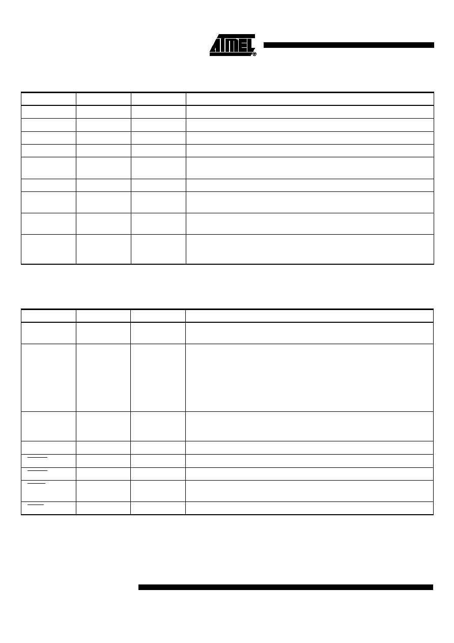
Notes:
1. MIDI and Audio group pins are powered by V
CC1
power rail.
2. These pins have alternate functions as GPIO pins (general-purpose input/output pins). See "General-purpose Input/Output
Routing" on page 24 for more details.
Table 3. MIDI and Audio Group
(1)
Name
Pin Count
Type
Function
MIDI1_IN
1
IN
Main MIDI input. Routed to PDSP#1, can also be routed to PDSP#2.
MIDI2_IN
1
I/O
Auxiliary MIDI input. Routed to PDSP#2
(2)
MIDI1_OUT
1
OUT
Main MIDI output. Outputs from PDSP#1.
MIDI2_OUT
1
OUT
Auxiliary MIDI output. Outputs from PDSP#2
(2)
OVCK_OUT
1
OUT
Buffered X2 output. Typically used to drive external sigma/delta DAC/ADC at
f
S
x 256.
BCK_OUT
1
OUT
Audio data bit clock. Provides timing to SD_OUT.
WS_OUT
1
OUT
Audio data word select. WS_OUT timing can be selected to be I2S- or
Japanese-compatible.
SD_OUT[7:0]
8
OUT
8 stereo serial audio data output (16 audio channels). Each output holds 64 bits
(2 x 32) of serial data per frame. Audio data has 22-bit precision
(2)
.
SD_IN[7:0]
8
I/O
8 stereo serial audio data input (16 audio channels). Each input holds 64 bits
(2 x 32) of serial data per frame. Audio data in is received with 20-bit
precision
(2)
.
Table 4. Memory Group
(1)
Name
Pin Count
Type
Function
CK_OUT
1
OUT
Master clock for SDRAM operation. Frequency is 4 times the X1 frequency
(typ 45.1584 MHz).
WA[26:0]
27
OUT
External memory address (ROM/SRAM/DRAM/SDRAM), up to 128M words
(256M bytes).
DRAM/SDRAM addresses are time-multiplexed on these pins as follows:
WA0 - WA8: DRA0 - DRA8
WA18: DRA9
WA20: DRA10
WA22: DRA11
RBS
1
OUT
SRAM byte select. Should be connected to the lower RAM address when 8-bit
wide SRAM is used. The type of RAM (16-bit/8-bit) can be selected by
program.
WD[15:0]
16
I/O
PCM ROM/SRAM/DRAM/SDRAM data
WCS0
1
OUT
PCM ROM chip select, active low
WCS1
1
OUT
SRAM chip select, active low
WWE
1
OUT
SRAM/DRAM/SDRAM write enable, active low. Timing compatible with SIMM
DRAM early write feature.
WOE
1
OUT
PCM ROM/SRAM output enable, active low
5
ATSAM9708
1772D≠DRMSD≠01/04
Note:
1. Memory group pins are powered by V
CC2
power rail.
Note:
1. X2 cannot be used to drive external circuitry.
RAS
1
I/O
DRAM/SDRAM row address strobe. At the end of reset RAS is tested to
determine memory type configuration (pulled high to select SDRAM type). RAS
should be pulled to V
CC
or GND through an external 10K resistor.
CAS
1
I/O
DRAM/SDRAM column address strobe. At the end of reset CAS is tested to
determine memory type configuration (pulled high to select DRAM type). CAS
should be pulled to V
CC
or GND through an external 10K resistor.
REFRESH
1
I/O
Indicates that a DRAM/SDRAM memory refresh cycle is in progress. To be
used with multiple SIMM/DIMM modules to force refresh simultaneously on all
modules. At the end of reset REFRESH is tested to select bootstrap state
(pulled high to start built-in CPU bootstrap in case of ROMless applications).
Table 5. Miscellaneous Group
Name
Pin Count
Type
Function
LFT
1
ANA
PLL low pass filter. Should be connected to an external RC network.
TEST
1
IN
Test pin. Should be returned to GND.
LDTEST
1
IN
Test pin. Should be returned to GND.
PDWN
1
IN
Power down, active low
RESET
1
IN
Master reset input, active low. Schmidt trigger input.
X1, X2
(1)
2
≠
Crystal connection. Crystal frequency should be f
S
x 256 (typ 11.2896 MHz).
Crystal frequency is internally multiplied by 4 to provide the IC master clock. X1
can also be used as external clock input (3.3V input).
Table 4. Memory Group
(1)
(Continued)
Name
Pin Count
Type
Function