 | –≠–ª–µ–∫—Ç—Ä–æ–Ω–Ω—ã–π –∫–æ–º–ø–æ–Ω–µ–Ω—Ç: T0980 | –°–∫–∞—á–∞—Ç—å:  PDF PDF  ZIP ZIP |
1
Features
∑
Power Amplifier with High Power Added Efficient (PAE),
P
out
Typically 29 dBm
∑
Controlled Output Power
∑
Low-noise Preamplifier (NF Typically 1.7 dB)
∑
Few External Components
∑
PSSO16 Plastic Package with Down Set Paddle
Description
The T0980 is a monolithic IC manufactured with Atmel's advanced SiGe technology.
The IC performs a transmit and receive front-end dedicated for a frequency range of
400 MHz to 500 MHz. It consists of a Low-Noise Amplifier (LNA) and a Power Ampli-
fier (PA) with good Power Efficiency (PAE).
Electrostatic sensitive device.
Observe precautions for handling.
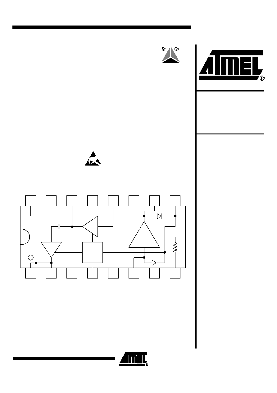
Figure 1. Block Diagram
16
13
11
9
1
3
5
8
Bias
SiGe Transmit/
Receive Front-
end IC
T0980
Rev. 4584A≠SIGE≠01/03

2
T0980
4584A≠SIGE≠01/03
Pin Configuration
Figure 2. Pinning PSSOP16
1
2
3
4
5
6
7
8
16
15
14
13
12
11
10
9
GND
POUT_
CONTROL
GND
LNA_IN
GND
BIAS_LNA
V2_PA_OUT
V2_PA_OUT
V1_PA
GND
PA_IN
GND
LNA_OUT
VS_CTRL
V2_PA_OUT
GND
T0980
Pin Description
Pin
Symbol
Function
1
V2_PA_OUT
Inductor to power supply and matching network for power amplifier output
2
V2_PA_OUT
Inductor to power supply and matching network for power amplifier output
3
GND
Ground
4
POUT_CONTROL
Power amplifier control input
5
GND
Ground
6
LNA_IN
Low-noise amplifier input
7
GND
Ground
8
BIAS_LNA
Resistor to V
S
sets the LNA current
9
VS_CTRL
Supply voltage for control of power amplifier
10
LNA_OUT
Low-noise amplifier output and supply voltage
11
GND
Ground
12
PA_IN
Power amplifier input
13
GND
Ground
14
V1_PA
Supply voltage for power amplifier
15
GND
Ground
16
V2_PA_OUT
Matching network for power amplifier output

3
T0980
4584A≠SIGE≠01/03
Absolute Maximum Ratings
All voltages are referred to GND
Parameters
Symbol
Min.
Max.
Unit
Supply voltage PA, TX Pins 1, 2, 9 and 14
V
S
_PA
4.8
V
Supply voltage LNA, RX Pin 10
V
S
_LNA
2.8
V
Junction temperature
T
jmax
150
∞
C
Storage temperature
T
Stg
-55
+125
∞
C
Electrostatic handling HMB; Pins 1, 2, 6, 10, 12 and 16
V
ESD
200
V
Electrostatic handling HMB; Pins 3, 4, 5, 7, 8, 9, 11, 13, 14 and 15
V
ESD
2000
V
Operating Range
All voltages are referred to GND. The following table represents the sum of all supply currents.
Parameters
Test Conditions/Pins
Symbol
Min.
Typ.
Max.
Unit
Supply voltage PA
TX, Pins 1, 2, 9 and 14
V
S
_PA
3.6
4.5
V
Supply voltage LNA
RX, Pin 10
V
S
_LNA
2.5
2.6
V
Supply current PA
TX, Pins 1, 2, 9 and 14
I
S
_PA
400
mA
Supply current LNA
Pins 10 and 8
I
S
_LNA
2.5
mA
Ambient temperature
T
amb
-25
25
60
∞
C
Thermal Resistance
Parameters
Symbol
Value
Unit
Junction ambient
R
thJA
25
K/W

4
T0980
4584A≠SIGE≠01/03
Note:
1. Power amplifier should be unconditional stable, maximum duty cycle 100%, true cw-operation, maximum load mismatch
10:1 for 5 s at 3.6 V
Electrical Characteristics
Test conditions (unless otherwise specified) : V
S
_PA = 3.6 V, T
amb
= 25
∞
C.
Parameters
Test Conditions/Pins
Symbol
Min.
Typ.
Max.
Unit
Power Amplifier
(1)
Supply voltage
TX, Pins 1, 2, 9 and 14
V
S
_PA
3.6
V
Supply current
TX, Pins 1, 2, 9 and 14
I
S
_PA
400
mA
Frequency range
TX
f
400
500
MHz
Power gain
TX
Gp
33
dB
Control voltage
TX, output power (maximum), Pin 4
2.5
V
TX, output power (minimum), Pin 4
0.7
V
Control current
Pin 4
0
400
µA
Shut down mode
Control voltage
£
0.1 V,
Pins 1, 2, 9 and 14
I
S
_PA
10
µA
Power added efficiency
TX at 450 MHz
PAE
50
%
Saturated output power
TX, input power 3 dBm
Psat
29
dBm
Harmonics
TX, input power 3 dBm
2 fo
-20
dBc
TX, input power 3 dBm
3 fo
-20
dBc
Low-noise Amplifier
Supply voltage
RX, Pins 8 and 10
V
S
_LNA
2.5
V
Supply current
RX at R1 = 5.6 k
W
, Pins 8 and 10
I
S
_LNA
2.5
mA
Frequency range
RX
f
400
500
MHz
Power gain
RX at R1 = 5.6 k
W
, Is = 2.5 mA
Gp
19
dB
Noise figure
RX at R1 = 5.6 k
W
, Is = 2.5 mA
NF
1.7
2.5
dB
Isolation
RX at R1 = 5.6 k
W
, Is = 2.5 mA
ISO
20
dB
3rd-order input interception point
RX at R1 = 5.6 k
W
, Is = 2.5 mA
IIP3
-10
dBm

5
T0980
4584A≠SIGE≠01/03
Typical Characteristics
Figure 3. Power Sweep
Figure 4. Ramp Sweep
Figure 5. V
CC
Sweep
-20.0
-10.0
0.0
10.0
20.0
30.0
40.0
50.0
60.0
70.0
-50.0
-40.0
-30.0
-20.0
-10.0
0.0
10.0
20.0
Pin (dBm)
PAE (%)
Pout (dBm)
G
a
in (dB)
Pout
Gain
PAE
0
10
20
30
40
50
60
70
0.00
0.50
1.00
1.50
2.00
2.50
3.00
3.50
Vramp (V)
PAE (%)
Pout (dBm)
Pout
PAE
0.0
10.0
20.0
30.0
40.0
50.0
60.0
70.0
0.0
1.0
2.0
3.0
4.0
5.0
V
CC
(V)
PAE (%)
Pout (dBm)
PAE
Pout