 | –≠–ª–µ–∫—Ç—Ä–æ–Ω–Ω—ã–π –∫–æ–º–ø–æ–Ω–µ–Ω—Ç: T2117-TAQ | –°–∫–∞—á–∞—Ç—å:  PDF PDF  ZIP ZIP |

T2117
Rev. A2, 17-Dec-01
1 (11)
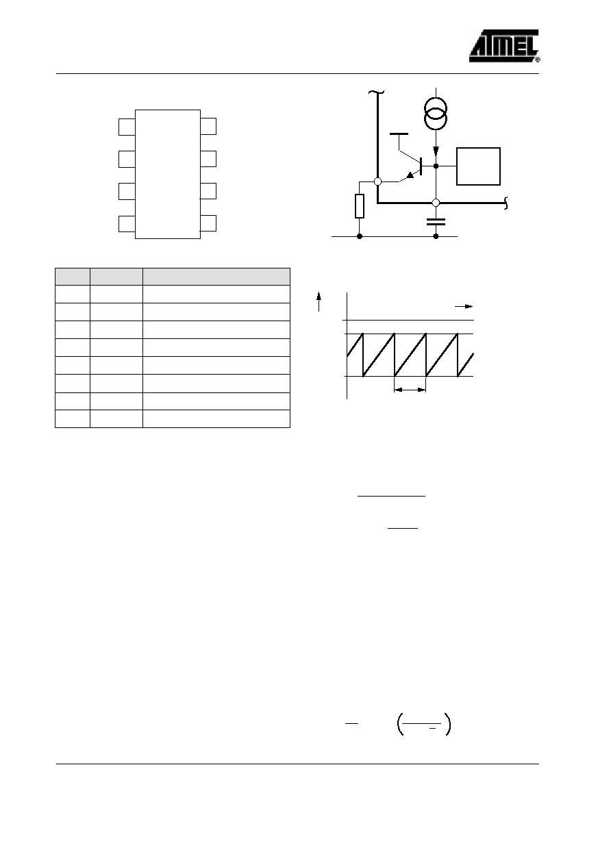
Zero-Voltage Switch with Adjustable Ramp
Description
The integrated circuit, T2117, is designed as a zero-
voltage switch in bipolar technology. It is used to control
resistive loads at mains by a triac in zero-crossing mode.
A ramp generator allows power control function by
period group control, whereas full-wave logic guarantees
that full mains cycles are used for load switching.
Features
D Direct supply from the mains
D Current consumption
0.5 mA
D Very few external components
D Full-wave drive ≠ no DC current component in the
load circuit
D Negative output current pulse typ. 100 mA ≠
short-circuit protected
D Simple power control
D Ramp generator
D Reference voltage
Applications
D Full-wave power control
D Temperature regulation
D Power blinking switch
Block Diagram
Ramp
generator
Pulse
amplifier
Comparator
R
1
18 k
W/
2 W
D
1
BYT41M
L
TIC
236N
Synchronization
Supply
Full-wave logic
+
≠
Reference voltage
1.4 V
1
3
4
R
4
100 k
W
2
8
5
C
2
2.2
mF/
10 V
R
5
12 k
W
min
max
100 k
W
R
6
18 k
W
7
6
220 k
W
C
1
100
W
R
3
Load
1000 W
V
M
=
230 V~
N
(R
sync
)
R
2
(250 V~)
MT2
MT1
GND
+
100
mF/
16 V
T2117
≠V
S
Figure 1. Block diagram with typical circuit, period group control 0 to 100%
Ordering Information
Extended Type Number
Package
Remarks
T2117-3AS
DIP8
Tube
T2117-TAS
SO8
Tube
T2117-TAQ
SO8
Taped and reeled
T2117
Rev. A2, 17-Dec-01
2 (11)
Pin Description
1
2
3
4
8
7
6
5
Ramp
C
Ramp
POSIN
NEGIN
V
sync
GND
Output
V
S
T2117
Figure 2. Pinning
Pin
Symbol
Function
1
Ramp
Ramp output
2
C
Ramp
Ramp capacitor
3
POSIN
Non-inverting comparator input
4
NEGIN
Inverting comparator input
5
V
S
Supply voltage
6
Output
Trigger pulse output
7
GND
Ground
8
V
sync
Voltage synchronization
General Description
The integrated circuit T2117 is a triac controller for zero-
crossing mode. It is designed to control power in
switching resistive loads of mains supplies.
Information regarding supply sync. is provided at Pin 8
via resistor R
Sync
. To avoid DC load on the mains, the full-
wave logic guarantees that complete mains cycles are
used for load switching.
A fire pulse is released when the inverting input of the
comparator is negative (Pin 4) with respect to the non-
inverting input (Pin 3) and internal reference voltage. A
ramp generator with free selectable duration can be
performed by capacitor C
2
at Pin 2. The ramp function is
used for open-loop control (figure 4), but also for applica-
tion with proportional band regulation (figure 11). Ramp
voltage available at capacitor C
2
is decoupled across the
emitter follower at Pin l. To maintain the lamp flicker
specification, ramp duration is adjusted according to the
controlling load. In practice, interference should be
avoided (temperature control). Therefore, a two-point
control is preferred to proportional control. One can use
internal reference voltage for simple applications. In that
case, Pin 3 is inactive and connected to Pin 7 (GND), see
figure 13.
Ramp
control
1
C
2
≠V
S
2
T2117
R
4
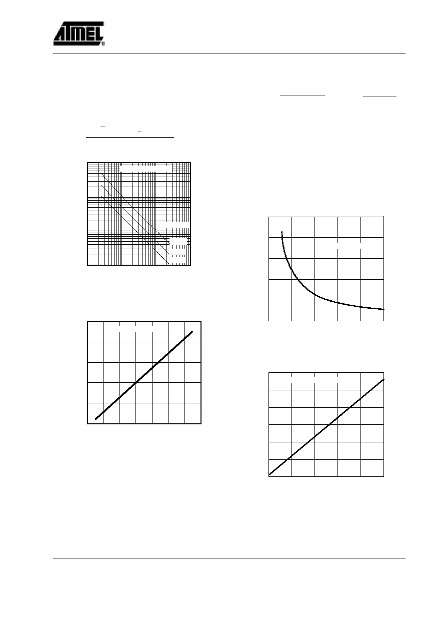
Figure 3. Pin 1 internal network
V
1
≠1.6 V
≠7.6 V
T
V
min
t
Final voltage
Initial voltage
V
max
Figure 4. Threshold voltage of the ramp at V
S
= ≠8.8 V
Triac Firing Current (Pulse)
This depends on the triac requirement. It can be limited
with gate series resistance which is calculated as follows:
R
Gmax
7.5 V ≠ V
Gmax
I
Gmax
≠ 36
W
I
P
=
I
Gmax
T
t
p
where:
V
G
= Gate voltage
I
Gmax
= Maximum gate current
I
p
= Average gate current
t
p
= Firing pulse width
T
= Mains period duration
Firing Pulse Width t
p
(Figure 5)
This depends on the latching current of the triac and its
load current. The firing pulse width is determined by the
zero-crossing detection which can be influenced with the
help of sync. resistance, R
sync
, (figure 6).
t
p
=
2
w
arc. sin
I
L
V
M
P 2
T2117
Rev. A2, 17-Dec-01
3 (11)
whereby:
I
L
=
Latching current of the triac
V
M
=
Mains supply, effective
P
=
Power load (user's power)
Total current consumption is influenced by the firing
pulse width which can be calculated as follows:
R
sync
+
V
M
2 sin (
w
tp
2
)
* 0.6 V
3.5
10
* 5
A
* 49 kW
0.01
0.10
1.00
10.00
10
100
1000
10000
t ( ms )
P ( W
)
p
I
L
( mA)
100
200
50
V
Mains
= 230 V
Figure 5. Output pulse width
0
400
800
1200
1600
2000
0
200
400
600
800 1000 1200 1400
Rsync ( kOhm )
tp (
ms )
V
Mains
= 230 V
Figure 6. Synchronization resistance
Supply Voltage
The T2117 contains voltage limiting and can be con-
nected with the mains supply via the diode D
1
and the
resistor R
1
. Supply voltage between Pin 5 and 7 is limited
to a typical value of 9.5 V.
The series resistance R
1
can be calculated (figures 7
and 8) as follows:
R
1max
= 0.85
V
Mmin ≠
V
Smax
2 I
tot
;
P
(R1)
=
(V
M ≠
V
S
)
2
2 R
1
I
tot
= I
S
+ I
P
+ I
x
whereby:
V
M
= Mains voltage
V
S
= Limiting voltage of the IC
I
tot
= Total current consumption
I
S
= Current requirement of the IC (without load)
I
x
= Current requirement of other peripheral
components
P
(R1)
= Power dissipation at R
1
0
3
6
9
12
0
10
20
30
40
50
R ( k )
1
I
tot
( mA )
15
V
Mains
=230V
X
W
Figure 7. Maximum resistance of R
1
0
3
6
9
12
0
I
tot
( mA )
15
V
Mains
=230V
X
1
2
3
4
6
P
(
W
)
5
R1
Figure 8. Power dissipation of R
1
according to current consumption

T2117
Rev. A2, 17-Dec-01
4 (11)
Absolute Maximum Ratings
Parameter
Symbol
Value
Unit
Supply current
Pin 5
≠I
S
30
mA
Sync. current
Pin 8
I
Sync.
5
mA
Output current ramp generator
Pin 1
I
O
3
mA
Input voltages
Pin 1, 3, 4, 6
Pin 2
Pin 8
≠V
I
≠V
I
±
V
I
V
S
2 to V
S
7.3
V
V
V
Power dissipation
T
b
= 45
∞
C
P
400
mW
T
amb
= 45
∞
C
T
amb
= 100
∞
C
P
tot
P
tot
400
125
mW
mW
Junction temperature
T
j
125
∞
C
Operating ambient temperature range
T
amb
0 to 100
∞
C
Storage temperature range
T
stg
≠40 to + 125
∞
C
Thermal Resistance
Parameter
Symbol
Value
Unit
Junction ambient
SO8
R
thJA
200
K/W
Junction ambient
DIP8
R
thJA
110
K/W
Electrical Characteristics
≠V
S
= 8.8 V, T
amb
= 25
∞
C, reference point Pin 7, unless otherwise specified
Parameter
Test Conditions / Pins
Symbol
Min.
Typ.
Max.
Unit
Supply-voltage limitation
≠I
S
= 1 mA
Pin 5
≠I
S
= 10 mA
Pin 5
≠V
S
≠V
S
9.0
9.1
9.5
9.6
10.0
10.1
V
V
Supply current
Pin 5
≠I
S
500
mA
Voltage limitation
I
8
=
±
1 mA
Pin 8
±
V
I
7.7
8.2
8.7
V
Synchronization current
Pin 8
±
I
sync
0.12
mA
Zero detector
Pin 8
±
I
sync
35
mA
Output pulse width
V
M
= 230 V
,
R
sync
= 220 k
W
Pin 6
R
sync
= 470 k
W
Pin 6
t
P
t
P
260
460
ms
ms
Output pulse current
V
6
= 0 V
Pin 6
≠I
O
100
mA
Comparator
Input offset voltage
Pin 3,4
±
V
I0
15
mV
Input bias current
Pin 4
I
IB
1
mA
Common-mode input
voltage
Pin 3,4
≠V
IC
1
(V
S
≠1)
V
Threshold internal
reference
V
3
= 0 V
Pin 4
≠V
Ref
1.4
V
T2117
Rev. A2, 17-Dec-01
5 (11)
Electrical Characteristics (continued)
≠V
S
= 8.8 V, T
amb
= 25
∞
C, reference point Pin 7, unless otherwise specified
Unit
Max.
Typ.
Min.
Symbol
Test Conditions / Pins
Parameter
Ramp generator, figure 1
Period
≠I
S
= 1 mA, i
sync
=1 mA,
C
1
= 100
mF, C
2
= 2.2
mF,
R
4
= 100 k
W
Pin 1
T
1.5
s
Final voltage
Pin 1
≠V
1
1.2
1.6
2.0
V
Initial voltage
Pin 1
≠V
1
7.2
7.6
8.0
V
Charge current
V
2
= ≠V
S
, I
8
= ≠1 mA, Pin 2
≠I
2
14
20
26
mA
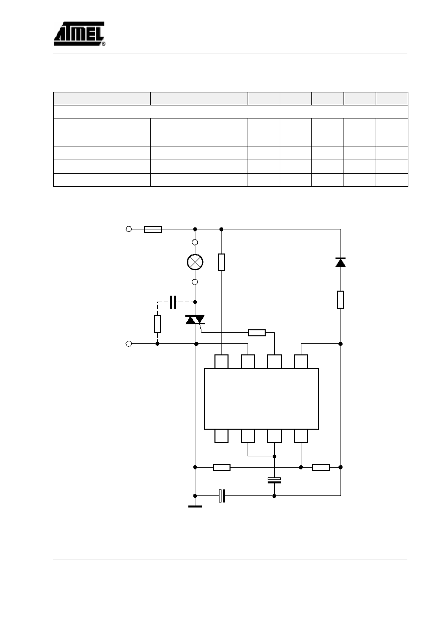
Applications
8
7
6
5
1
2
3
4
T2117
270 k
W
V
M
= 230 V ~
56
W
BYT41M
18 k
W/
1.5 W
L
N
100 nF/
250 V ~
82
W
0.5 ...
2.2 kW
110 k
W
150 k
W
47
mF/ 16V
0.47
mF/
10 V
Figure 9. Power blinking switch with f
2.7 Hz, duty cycle 1:1, power range 0.5 to 2.2 kW