1
Features
∑
No External Components Except PIN Diode
∑
Supply-voltage Range: 4.5 V to 5.5 V
∑
Automatic Sensitivity Adaptation (AGC)
∑
Automatic Strong Signal Adaptation (ATC)
∑
Enhanced Immunity Against Ambient Light Disturbances
∑
Available for Carrier Frequencies between 30 kHz to 76 kHz; Adjusted by Zener Diode
Fusing
∑
TTL and CMOS Compatible
∑
Suitable Minimum Burst Length
6 or 10 Pulses/Burst
Applications
∑
Audio Video Applications
∑
Home Appliances
∑
Remote Control Equipment
Description
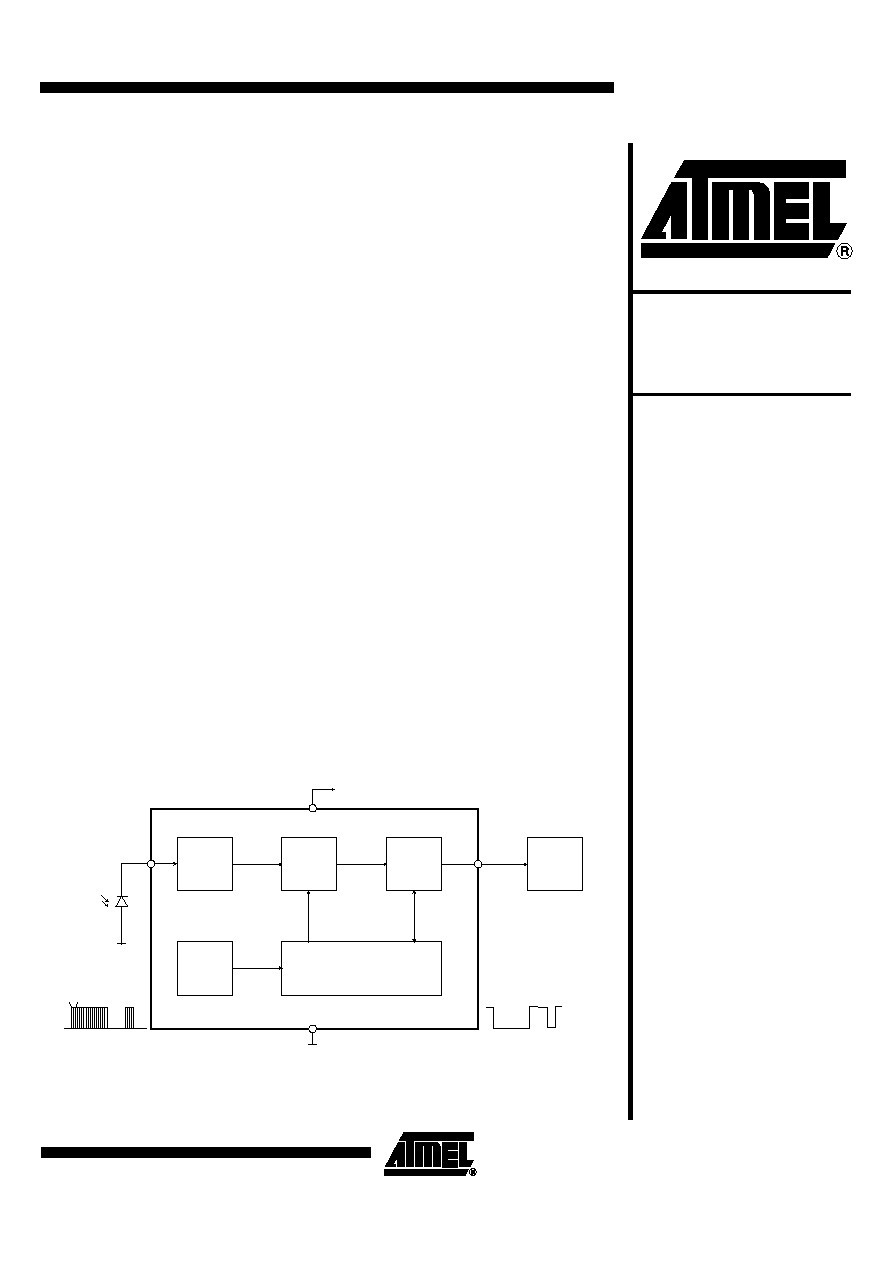
The IC T2525 is a complete IR receiver for data communication developed and opti-
mized for use in carrier-frequency-modulated transmission applications. Its function
can be described using the block diagram (see Figure 1). The input stage meets two
main functions. First, it provides a suitable bias voltage for the PIN diode. Secondly,
the pulsed photo-current signals are transformed into a voltage by a special circuit
which is optimized for low-noise applications. After amplification by a
controlled gain
amplifier (CGA), the signals have to pass a tuned integrated narrow bandpass filter
with a center frequency f
0
which is equivalent to the chosen carrier frequency of the
input signal. The demodulator is used to convert the input burst signal into a digital
envelope output pulse and to evaluate the signal information quality, i.e., unwanted
pulses will be suppressed at the output pin. All this is done by means of an integrated
dynamic feedback circuit which varies the gain as a function of the present environ-
mental condition (ambient light, modulated lamps etc.). Other special features are
used to adapt to the current application to secure best transmission quality. The
T2525 operates in a supply-voltage range of 4.5 V to 5.5 V.
Figure 1. Block Diagram
Input
µC
CGA and
filter
Demodulator
Oscillator
AGC/ATC and digital
control
VS
Modulated IR signal
min 6/10 pulses
GND
IN
OUT
Carrier frequency f0
IR Receiver
ASSP
T2525
Rev. 4657A≠AUTO≠01/03

2
T2525
4657A≠AUTO≠01/03
Pin Configuration
Figure 2. Pinning SO8 and TSSOP8
1
2
3
4
8
7
6
5
VS
n.c.
OUT
n.c.
n.c.
n.c.
GND
IN
Pin Description
Pin
Symbol
Function
1
VS
Supply voltage
2
n.c.
Not connected
3
OUT
Data output
4
n.c.
Not connected
5
IN
Input PIN-diode
6
GND
Ground
7
n.c.
Not connected
8
n.c.
Not connected
Absolute Maximum Ratings
Parameter
Symbol
Value
Unit
Supply voltage
V
S
-0.3 to +6
V
Supply current
I
S
3
mA
Input voltage
V
IN
-0.3 to V
S
V
Input DC current at V
S
= 5 V
I
IN
0.75
mA
Output voltageV
O
-0.3 to V
S
V
V
O
-0.3 to V
S
V
Output current
I
O
mA
Operating temperature
T
amb
∞C
Storage temperature
T
stg
∞C
Power dissipation at T
amb
= 25∞C
P
tot
30
mW
Thermal Resistance
Parameter
Symbol
Value
Unit
Junction ambient SO8
R
thJA
130
k/W
Junction ambient TSSOP8
R
thJA
tbd
K/W
3
T2525
4657A≠AUTO≠01/03
Electrical Characteristics
Tamb = -25 to 85∞C, VS = 4.5 to 5.5
V unless otherwise specified.
No.
Parameters
Test Conditions
Pin
Symbol
Min.
Typ.
Max.
Unit
Type*
1
Supply
1.1
Supply-voltage range
1
V
S
4.5
5
5.5
V
C
1
.
2
Supply current
I
IN
=0
1
I
S
0.8
1.1
1.3
mA
B
2
Output
2.1
Internal pull-up
resistor
1)
T
amb
= 25∞C;
see Figure 9
1,3
R
PU
30/40
kW
A
2.2
Output voltage low
I
L
= 2 mA;
see Figure 9
3,6
V
OL
250
mV
B
2.3
Output voltage high
3,1
V
OH
V
S
-
0.25
Vs
V
B
2.4
Output current
clamping
R
2
= 0; see Figure 9
3,6
I
OCL
8
mA
B
3
Input
3.1
Input DC current
V
IN
= 0; see Figure 9
5
I
IN_DCMAX
-85
µA
C
3.2
Input DC-current;
Figure 4
V
IN
= 0; V
s
= 5 V,
T
amb
= 25∞C
5
I
IN_DCMAX
-530
-960
µA
B
3.3
Minimum detection
threshold current;
Figure 3
Test signal:
see Figure 8
V
S
= 5 V,
T
amb
= 25∞C,
I
IN_DC
= 1µA;
square pp,
burst N = 16,
f = f
0
; t
PER
= 10 ms,
Figure 8;
BER = 50
2)
3
I
Eemin
-520
pA
B
3.4
Minimum detection
threshold current with
AC current
disturbance
IIN_AC100 = 3 µA at
100 Hz
Test signal:
see Figure 8
V
S
= 5 V,
T
amb
= 25∞C,
I
IN_DC
= 1 µA,
square pp,
burst N = 16,
f = f
0
; t
PER
= 10 ms,
Figure 8;
BER = 50%
2)
3
I
Eemin
-800
pA
C
*) Type means: A =100% tested, B = 100% correlation tested, C = Characterized on samples, D = Design parameter
Note:
1. Depending on version, see "Ordering Information"
2. BER = bit error rate; e.g., BER = 5% means that with P = 20 at the input pin 19...21 pulses can appear at the Pin OUT
3. After transformation of input current into voltage

4
T2525
4657A≠AUTO≠01/03
ESD
All pins
Þ
2000V HBM; 200V MM, MIL-STD-883C, Method 3015.7
Reliability
Electrical qualification (1000h) in molded S08 plastic package
3.5
Maximum detection
threshold current with
V
IN
> 0V
Test signal:
see Figure 8
V
S
= 5V, T
amb
= 25∞C,
I
IN_DC
= 1µA;
square pp,
burst N = 16,
f = f
0
; t
PER
= 10ms,
Figure 8; BER = 5%
2)
3
I
Eemax
-400
µA
D
4
Controlled Amplifier and Filter
4.1
Maximum value of
variable gain (CGA)
G
VARMAX
51
dB
D
4.2
Minimum value of
variable gain (CGA)
G
VARMIN
-5
dB
D
4.3
Total internal
amplification
3)
G
MAX
71
dB
D
4.4
Center frequency
fusing accuracy of
bandpass
V
S
= 5 V, T
amb
= 25∞C
f
0_FUSE
-3
f
0
+3
%
A
4.5
Overall accuracy
center frequency of
bandpass
f
0
-6.7
f
0
+4.1
%
C
4.6
BPF bandwidth:
type N0 - N3
BPF bandwidth:
type N6, N7
-3 dB; f
0
= 38 kHz;
see Figure 6
-3 dB; f
0
= 38 kHz
B
B
3.5
5.4
kHz
kHz
C
C
Electrical Characteristics (Continued)
Tamb = -25 to 85∞C, VS = 4.5 to 5.5
V unless otherwise specified.
No.
Parameters
Test Conditions
Pin
Symbol
Min.
Typ.
Max.
Unit
Type*
*) Type means: A =100% tested, B = 100% correlation tested, C = Characterized on samples, D = Design parameter
Note:
1. Depending on version, see "Ordering Information"
2. BER = bit error rate; e.g., BER = 5% means that with P = 20 at the input pin 19...21 pulses can appear at the Pin OUT
3. After transformation of input current into voltage
5
T2525
4657A≠AUTO≠01/03
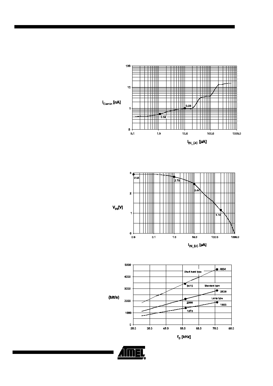
Typical Electrical Curves at T
amb
= 25∞C
Figure 3. I
Eemin
versus I
IN_DC
, V
S
= 5 V
Figure 4. V
IN
versus I
IN_DC
, V
S
= 5 V
Figure 5. Data Transmission Rate, V
S
= 5 V