1
Features
∑
Low-power, Low-voltage Operation
∑
Contactless Power Supply
∑
Contactless Read/Write Data Transmission
∑
Radio Frequency (RF): 100 kHz to 150 kHz
∑
264-bit EEPROM Memory in 8 Blocks of 33 Bits
∑
224 Bits in Seven Blocks of 32 Bits are Free for User Data
∑
Block Write Protection
∑
Extensive Protection Against Contactless Malprogramming of the EEPROM
∑
On-chip Resonance Capacitor (70 or 200 pF Mask Option)
∑
Anticollision Using Answer-On-Request (AOR)
∑
Typical < 50 ms to Write and Verify a Block
∑
Other Options Set by EEPROM:
≠ Bitrate [bit/s]: RF/8, RF/16, RF/32, RF/40, RF/50, RF/64, RF/100, RF/128
≠ Modulation: BIN, FSK, PSK, Manchester, Biphase
≠ Other: Terminator Mode, Password Mode, AOR Mode
Description
The T5554 is a contactless R/W-
IDentification IC (IDIC
“
) for general-purpose applica-
tions in the 125 kHz range. A single coil, connected to the chip, serves as the IC's
power supply and bidirectional communication interface. The coil and chip together
form a transponder.
The on-chip 264-bit EEPROM (8 blocks 33 bits each) can be read and written block-
wise from a base station. The blocks can be protected against overwriting. One block
is reserved for setting the operation modes of the IC. Another block can contain a
password to prevent unauthorized writing.
Reading occurs by damping the coil by an internal load. There are different bitrates
and encoding schemes possible. Writing occurs by interrupting the RF field in a spe-
cial way.
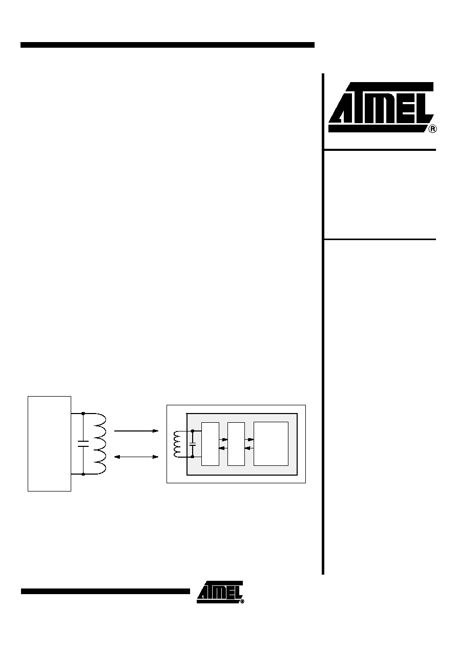
System Block Diagram
Figure 1. RFID System Using T5554 Tag
C
o
n
t
r
o
l
l
e
r
C
o
i
l
i
n
t
e
r
f
a
c
e
Memory
Transponder
Base station
Data
Power
C
o
n
t
r
o
l
l
e
r
C
o
i
l
i
n
t
e
r
f
a
c
e
Memory
Transponder
Base station
Data
T5554
Power
Standard R/W
IDIC (264 Bit)
with Integrated
Capacitance
T5554
Preliminary
Rev. 4576A≠RFID≠12/02
2
T5554
4576A≠RFID≠12/02
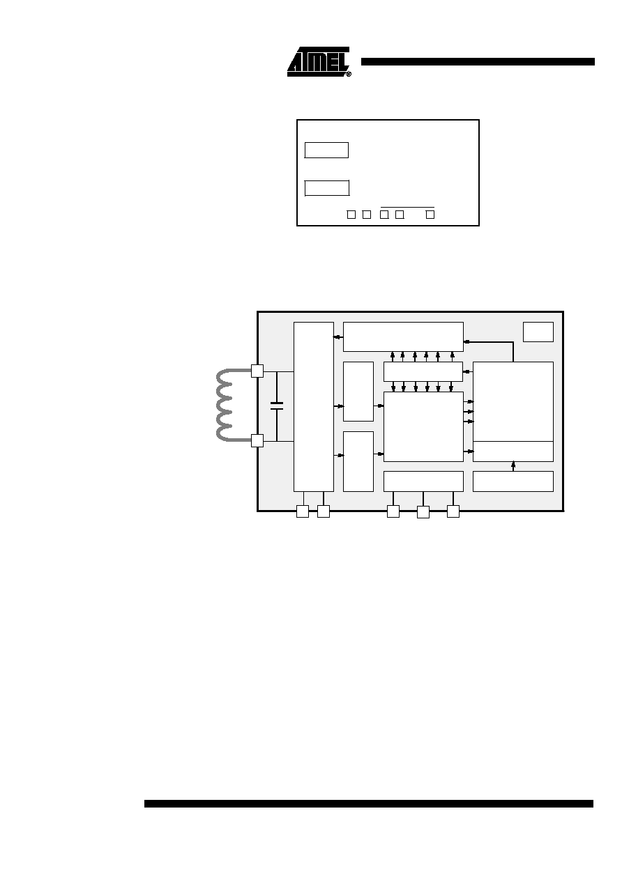
Pad Layout
Figure 2. Pad Layout of T5554
T5554 Building Blocks
Figure 3. Block Diagram
Analog Front End (AFE)
The AFE includes all circuits which are directly connected to the coil. It generates the
IC's power supply and handles the bidirectional data communication with the reader
unit. It consists of the following blocks:
∑
Rectifier to generate a DC supply voltage from the AC coil voltage
∑
Clock extractor
∑
Switchable load between Coil1/Coil2 for data transmission from the IC to the reader
unit (read)
∑
Field gap detector for data transmission from the reader unit into the IC (write)
Resonance Capacitor
The resonance capacitor is integrated on chip. By mask option the value can be 70 pF
or 200 pF typically.
Coil 1
Coil 2
V
V
Test pads
DD
SS
T5554
Coil 1
Coil 2
Modulator
A
n
a
l
o
g
f
r
o
n
t
e
n
d
POR
Input register
W
r
i
t
e
d
e
c
o
d
e
r
B
i
t
r
a
t
e
g
e
n
e
r
a
t
o
r
Memory
(264 bit EEPROM)
Controller
Test logic
Mode register
HV generator
VDD VSS
Test pads

3
T5554
4576A≠RFID≠12/02
Controller
The main controller has the following functions:
∑
Load mode register with configuration data from EEPROM block 0 after power-on
and also during reading
∑
Control memory access (read, write)
∑
Handle write data transmission and the write error modes
∑
The first two bits of the write data stream are the OP-code. There are two valid OP-
codes (standard and stop) which are decoded by the controller.
∑
In password mode, the 32 bits received after the OP-code are compared with the
stored password in block 7.
Bitrate Generator
The bitrate generator can deliver the following bitrates:
RF/8 ≠ RF/16 ≠ RF/32 ≠ RF/40 ≠ RF/50 ≠ RF/64 ≠ RF/100 ≠ RF/128
Write Decoder
Decode the detected gaps during writing. Check if write data stream is valid.
Test Logic
Test circuitry allows rapid programming and verification of the IC during test.
HV Generator
Voltage pump which generates
~
18 V for programming of the EEPROM.
Power-On Reset (POR)
The power-on reset is a delay reset which is triggered when supply voltage is applied.
Mode Register
The mode register stores the mode data from EEPROM block 0. It is continually
refreshed at the start of every block. This increases the reliability of the device (if the
originally loaded mode information is false, it will be corrected by subsequent refresh
cycles).
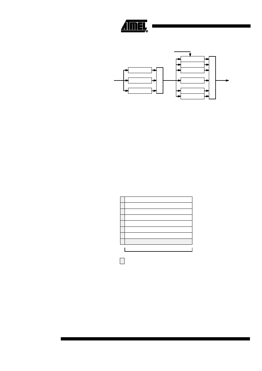
Modulator
The modulator consists of several data encoders in two stages, which may be freely
combined to obtain the desired modulation. The basic types of modulation are:
∑
PSK: phase shift: 1) every change; 2) every "1"; 3) every rising edge (carrier: fc/2,
fc/4 or fc/8)
∑
FSK: 1) f1 = rf/8 f2 = rf/5; 2) f1 = rf/8, f2 = rf/10
∑
Manchester: rising edge = H; falling edge = L
∑
Biphase: every bit creates a change, a data "H" creates an additional mid-bit change
Note:
The following modulation type combinations will not work:
∑
Stage1 Manchester or Biphase and stage2 PSK, at any PSK carrier frequency
(because the first stage output frequency is higher than the second stage strobe
frequency);
∑
Stage1 Manchester or Biphase and stage2 PSK with bitrate = rf/8 and PSK carrier
frequency = rf/8 (for the same reason as above);
∑
Any stage1 option with any PSK for bitrates rf/50 or rf/100 if the PSK carrier
frequency is not an integer multiple of the bitrate (e.g., br = rf/50, PSKcf = rf/4,
because 50/4 = 12.5). This
i
s because the PSK carrier frequency must maintain
constant phase with respect to the bit clock.
4
T5554
4576A≠RFID≠12/02
Figure 4. Modulator Block Diagram
Memory
The memory of the T5554 is a 264-bit EEPROM, which is arranged in 8 blocks of 33 bits
each. All 33 bits of a block, including the lock bit, are programmed simultaneously. The
programming voltage is generated on-chip.
Block 0 contains the mode data, which are not normally transmitted (see figure 6).
Blocks 1 to 6 are freely programmable. Block 7 may be used as a password. If password
protection is not required, it may be used for user data.
Bit 0 of every block is the lock bit for that block. Once locked, the block (including the
lockbit itself) cannot be field-reprogrammed.
Data from the memory is transmitted serially, starting with block 1, bit 1, up to block
"MAXBLK", bit 32. "MAXBLK" is a mode parameter set by the user to a value between 0
and 7 (if maxblk = 0, only block 0 will be transmitted).
Figure 5. Memory Map
Direct
Manchester
Biphase
PSK1
PSK2
PSK3
Direct
FSK1, 1a
FSK2, 2a
From memory
To load
Carrier frequency
Mux
Mux
1
0
32
L
L
L
L
L
L
L
L
Block 7
Block 6
Block 5
Block 4
Block 3
Block 2
Block 1
Block 0
User data or password
32 bits
User data
User data
User data
User data
User data
User data
Configuration data
Not transmitted
5
T5554
4576A≠RFID≠12/02
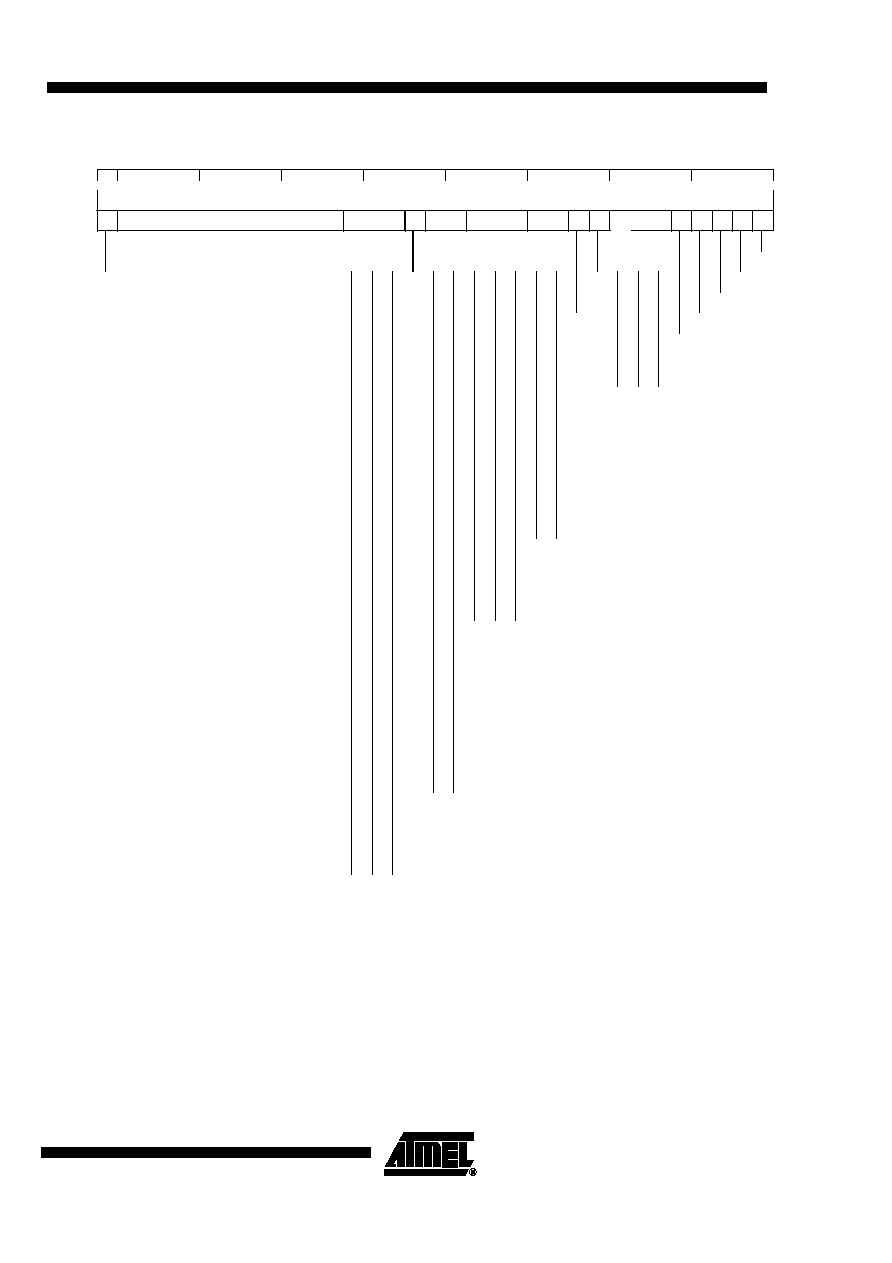
Figure 6. Memory Map of Block 0
0
1
MAXBLK
32
reserved
11
25
27
15
[2] [1] [0]
MS2
18
20
[2] [1] [0]
MS1
16 17
[1] [0]
31
30
29
28
24
23
22
[1] [0]
BR
12
14
[2] [1] [0]
res'd
*useSTOP
useBT
AOR
"0"
useST
send blocks:
usePWD
Key:
-----------------------------------
--
AOR Anwer-On-Request
BT use Block Terminator
ST use Sequence Terminator
PWD use Password
STOP obey stop header (active low!)
BR Bit Rate
MS1 Modulator Stage 1
MS2 Modulator Stage 2
PSKCF PSK Clock Frequency
MAXBLK see Maxblock feature
reserved do not use
* Bit 15 and 24 must always be at "0",
otherwise malfunction will appear.
lock bit (never transmitted)
PSKCF
21
26
19
13
0 0 0 0
0 0 1 1
0 1 0 1 to 2
0 1 1 1 to 3
1 0 0 1 to 4
1 0 1 1 to 5
1 1 0 1 to 6
1 1 1 1 to 7
0 0 RF/2
0 1 RF/4
1 0 RF/8
1 1 reserved
0 0 0 direct
0 0 1 psk1 (phase change when input changes)
0 1 0 psk2 (phase change on bitclk if input high)
0 1 1 psk3 (phase change on rising edge of input)
-----------------------------------
o/p freq. DATA=1 DATA=0
1 0 0 fsk1 rf/8 rf/5
1 0 1 fsk2 rf/8 rf/10
1 1 0 fsk1a rf/5 rf/8
1 1 1 fsk2a rf/10 rf/8
0 0 direct
0 1 Manchester
1 0 Biphase
1 1 reserved
0 0 0 RF/8 bitrate_8cpb
0 0 1 RF/16 bitrate_16cpb
0 1 0 RF/32 bitrate_32cpb
0 1 1 RF/40 bitrate_40cpb
1 0 0 RF/50 bitrate_50cpb
1 0 1 RF/64 bitrate_64cpb
1 1 0 RF/100 bitrate_100cpb
1 1 1 RF/128 bitrate_128cpb
"0"
*
*