Rev. 4761A≠AUTO≠11/03
Features
∑
Input Comparator with Schmitt-trigger Characteristic
∑
Input Clamping Current Capability of ±10 mA
∑
Integrated Protection Cells (EMC, ESD, RF) Dedicated to All Input Stages
∑
Shutdown by Junction-temperature Monitor
∑
Reset with Hysteresis at Low Voltage
∑
ESD Protection Acording to Human Body Model:
±2000 V (C = 100 pF, R = 1.5 k
)
∑
Output Stage:
≠ Short-circuit Protected
≠ Load-dump Protected at 1 k
≠ Jump Start Possible
Description
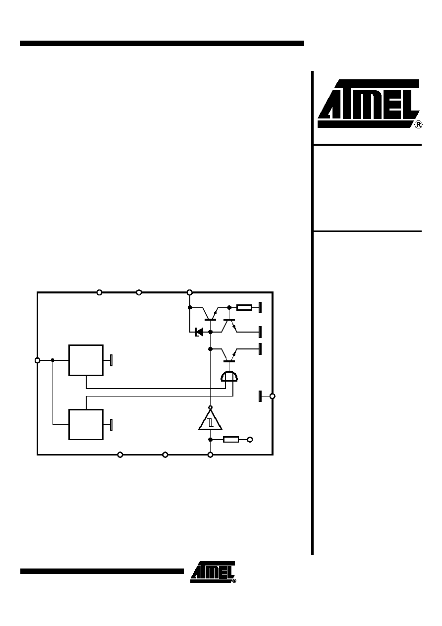
The singel-channel driver IC includes one non-inverted and current-limited output
stage with an open collector. Thermal shutdown protects the output against critical
junction temperatures. The output can sink a current of 20 mA. The digital input has
Schmitt-trigger function with pull-up resistors to 5 V.
Figure 1. Block Diagram
Under-
voltage
detection
7
1
3
NC
4
5
2
NC
V
O
V
S
NC
NC
V
I
GND
Thermal
shutdown
V
S
Single-channel
Driver IC with
Thermal
Monitoring
T6801
3
T6801
4761A≠AUTO≠11/03
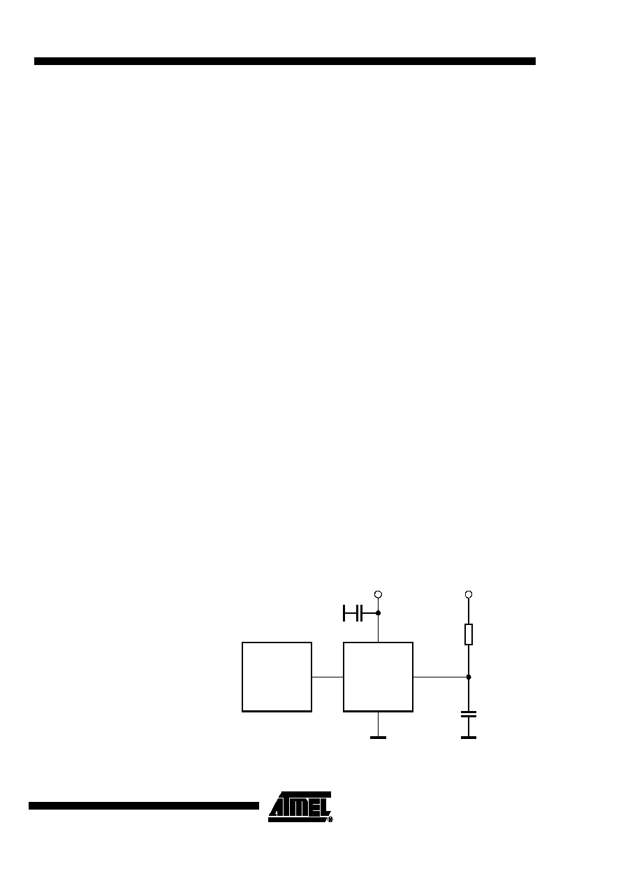
Basic Circuitry
The integrated circuit T6801 requires a stabilized supply voltage (V
S
= 5 V ±5%) to com-
ply with its electrical characteristics. An external buffer capacitor of C = 100 nF is
recommended. An integrated 14 V Zener diode between V
S
and ground protects the
supply pin.
The input stage is provided with an integrated 250 k
W
pull-up resistor and can be
directly connected to a microcontroller.
The output stage is an open collector, capable of sinking 20 mA. Recommended exter-
nal components:
∑
Pull-up resistor, R = 1 k
W
∑
Capacitor to GND, C = 470 pF, see Figure 3
Functional Description
General
ON state: Low level at the input stage activates the output stage.
OFF state: The internal pull-up resistor provides high level to the input comparator and
deactivates the output stage.
A 7 V Zener diode between input pin and GND is capable of ±10 mA clamping current.
Current Limitation of the
Output Stages and
Overtemperature
Shutdown
A temperature-dependent current limitation in the range of 25 to 100 mA protects the
stage in case of a short circuit. Additionally, the chip temperature is monitored. For
T
Chip
> 148
∞
C, the output is disabled and automatically enabled with a hysteresis of
T
Chip
> 5
∞
C.
Transients and Load
Dump
An integrated 28 V Zener diode protects the output stage against transients and load-
dump (Schaffner pulses). With the help of an external 1 k
W
resistor, the output transistor
is capable of handling the corresponding current which flows during each of these condi-
tions. Apart from that, the output is short-circuit and overload protected.
Low-voltage Detection
When the supply voltage is switched on, a power-on reset pulse is generated internally
which disables the output stage until a defined supply-voltage level is reached. The low-
voltage detection is provided with a hysteresis of V
hyst
= 0.5 V typically.
Figure 3. Application Schematic
V
S
= 5 V
V
I
V
O
C
R
V
Batt
1 k
470 pF
Load
100 nF
Micro-
controller
T6801

4
T6801
4761A≠AUTO≠11/03
Absolute Maximum Ratings
Stresses beyond those listed under "Absolute Maximum Ratings" may cause permanent damage to the device. This is a stress rating
only and functional operation of the device at these or any other conditions beyond those indicated in the operational sections of this
specification is not implied. Exposure to absolute maximum rating conditions for extended periods may affect device reliability.
Parameters
Symbol
Value
Unit
Supply voltage
V
S
7.0
V
Ambient temperature range
T
amb
-40 to +125
∞
C
Storage temperature range
T
stg
-50 to +150
∞
C
Maximum junction temperature
T
j
+150
∞
C
Thermal Resistance
Parameters
Symbol
Value
Unit
Junction ambient
R
thJA
160
K/W
Electrical Characteristics
V
S
= 5 V ±5%, T
amb
= 27
∞
C, reference point pin 2 (GND), unless otherwise specified, see Figure 1 on page 1 and Figure 3
on page 3.
Parameters
Test Conditions
Symbol
Min.
Typ.
Max.
Unit
Supply, Pin 7
Supply voltage
V
S
4.75
5.25
V
Supply current
Input open
Input closed to GND
I
S
I
S
0.8
7
3.2
13
mA
mA
Low-voltage detection threshold
ON
OFF
V
TH(ON)
V
TH(OFF)
3.7
3.0
4.6
3.8
V
V
Low-voltage hysteresis
V
hyst
0.55
1.05
V
Temperature shutdown
T
Chip
140
149
∞
C
Temperature shutdown hysteresis
T
hyst
5
∞
C
Input, Pin 5
Zener-diode protection voltage
I
I
= 10 mA
V
I
6.7
8.5
V
Zener-diode clamping current
I
I
±10
mA
Pull-up resistor
R
I
170
250
305
k
W
Switching threshold
OFF
ON
V
I
V
I
3.3
1.8
V
V
Hysteresis
V
hyst
1.5
V
Output, Pin 4
Zener-diode protection voltage
I
O
= 10 mA
V
O
26.5
V
Integrated capacitor
5
pF
Leakage current
I
Leak
2.5
µA
Saturation voltage
(I
O
= 20 mA)
V
Sat
0.7
V
Current limitation
I
limit
25
100
mA
Propagation delay
(470 pF, 1 k
W
, 20 V)
t
d
5
µs