
Rev. A ≠ 27-Aug.-01
1
Features
∑
Besides the serial IEEE-1355 link, the T7906E provides several different interface
types:
≠ Host interface
The host interface provides 8 multiplexed data and address lines to program
and control the T7906E locally
≠ FIFO interface
The FIFO interface provides the control signals FULL, WRITE, EMPTY and READ
depending on the direction of the data flow (receive / transmit)
≠ ADC interface
The ADC interface allows to connect an ADC with a width of up to 16 bits directly
to the T7906E
≠ DAC interface
The DAC interface provides up to 16 bits data lines and the required control
signals. The data to be sent to the DAC are stored until a command "start DAC"
is received
≠ RAM interface
The RAM interface provides a 16-bit data bus and a 16-bit address bus. Four
chip select allow to address 4 different memory partitions. The memory interface
can be programmed to use up to 7 wait states
≠ UART interface
Two independent UART interfaces are included. One UART uses dedicated I/O
lines whereas the second UART is sharing its pins with the GPIO port
≠ General purpose I/O
This general Purpose Interface provides up to 24 bidirectional signal lines. The
direction of each GPIO line can be set individually via register
≠ Timer / Event Counter
Two 32-Bit on-chip timers are available. Each timer provides a 32-Bit counter
and a 32-Bit reload register. The two timers can be operated independently or
cascaded
≠ JTAG (IEEE 1149.1)
For testing purposes, a standard IEEE 1149.1 interface is provided. It supports
the JTAG function Bypass, Extest, Sample/preload, All-tristate and IDCode
∑
Designed on Atmel MG1090E sea of gates matrix and packaged into MQFPF100
∑
Also called SMCS Lite (or SMCS116)
Description
The T7906E provides one IEEE-1355 serial communication link with 0 to 200 Mbit/s
data transmit rate. It supports both the standard IEEE-1355 link protocol (transparent
mode) as well as the header generation required for the enhanced transaction layer of
the TSS901E. This protocol uses specific protocol headers that can be generated by
the T7906E without requiring an external host controller. These headers are stored in
specific header registers which allows headers with a length of 0 (equaling the trans-
parent mode) to eight bytes per packet. Packetization of data sent by the T7906E over
the link is also done automatically according to the settings of a packet length register.
Another feature provided by the transaction layer supported by the T7906E is an auto-
matic checksum generation on the link. This is generated and checked automatically
by the T7906E without requiring support from a host or other external source. Errors
on the link are flagged and a special error packet is sent over the link to signal the
error condition.
Programming the T7906E internal registers is done via the IEEE-1355 link. All internal
registers are 8-bit wide addressable. Two simple commands (read and write) suffice
to access all functions and registers of the T7906E.
Single Point to
Point IEEE 1355
High Speed
Controller
T7906E

2
T7906E
Rev. A ≠ 27-Aug.-01
The interfaces of the T7906E such as the FIFO, UART, ADC/DAC and memory inter-
face are accessed by a simple read or write operation to the corresponding interface
address. In the case of FIFO, Host, UART and memory interface, a packet oriented
access is also possible (meaning transferring multiple bytes with a single command). In
case a communication memory
is connected to the T7906E, this can be read and written to via the link specific registers.
The IEEE-1355 links can support a range of communication speeds, which are pro-
grammed by writing to registers. At reset all links are configured to run at the base
speed of 10 Mbits/sec. Only the transmission speed of a link is programmed as recep-
tion is asynchronous. This means that links running at different speeds can be
connected, provided that each device is capable of receiving at the speed of the con-
nected transmitter.
Introduction
Connecting a non-intelligent node to a processing element requires not only the commu-
nication controller, but usually a controlling instance for the communication circuitry. The
latter has to be configured for settings like bit rate, packet sizes, handshake protocols
etc. Should the non-intelligent node require remote control via commands, usually a
second link, dedicated for commands is introduced. Using an IEEE-1355 link for that
purpose eliminates the need for separate data and control paths, since the communica-
tion controller can differentiate between the two entities. In addition, it can be remotely
configured, can execute simple commands and provides special I/O pins to control the
interface unit.
The T7906E provides one IEEE-1355 serial communication link together with additional
features to support non-intelligent nodes as well as to control ADC and DAC converters.
The T7906E is targeted at two main applications areas:
∑
Embedded systems
∑
Communication device for processor systems
Embedded systems
The main application targets of the T7906E are modules and units without any built-in
communication features, such as special image compression chips, application specific
programmable logic or mass memory. The T7906E is perfectly suited to be used on
"non-intelligent" modules such as A/D-converter or sensor interfaces, due to its "control
by link" feature and system control facilities. In addition, its fault tolerance feature make
the device very interesting for many critical industrial measurement and control systems.
Example applications of the T7906E as communication and system controller on an
interface node consisting of an ADC and DAC and one where the T7906E is connected
to four banks of memory are given in the figures below:

3
T7906E
Rev. A ≠ 27-Aug.-01
Figure 1. Example applications

4
T7906E
Rev. A ≠ 27-Aug.-01
Communication device for microprocessors
Many applications require a link front end providing one link, but no controller instance
on that unit. Due to the communication memory interface of the SMCSlite, it is also sat-
isfying the requirements of these applications. Due to its small package and low power
consumption it is an excellent alternative to FPGA based solutions. A system using the
SMCSlite as a communication front-end for a microcontroller is shown in the figure
below:
Figure 2. Example application
Interfaces
FIFO interface
The FIFO interface provides the control signals full, write, empty and read, depending
on the direction of the data flow (receive/transmit).
Data received from the FIFO interface is sent over the IEEE-1355 link grouped in pack-
ets. The length of a packet (in bytes) can be specified either by setting an internal
counter or by external signals. This interface can be programmed to use 0 to 7 wait
states.
ADC/DAC interface
The ADC interface allows to connect an ADC with a width of up to 16 bits directly to the
T7906E. The AD conversion can be started by request via link or in a cyclic manner trig-
gered by the on-chip timers. When the AD conversion is ready, this is recognized by an
external signal like "ready" or by an internal trigger, for example from the on-chip timer.
After reading the sample from the ADC it is then sent over the link. An 8-bit address gen-
erator is provided to allow multiplexing of analog signals. The address generator will
start at a pre-programmed start address and will be incremented after each conversion.
The DAC interface is very similar to the ADC interface. It provides up to 16 data lines
and the required control signals. The data to be sent to the DAC is received from the link
and is stored in a register until the command "start DAC" is received. After that com-
mand the register values will be put to the DAC.
5
T7906E
Rev. A ≠ 27-Aug.-01
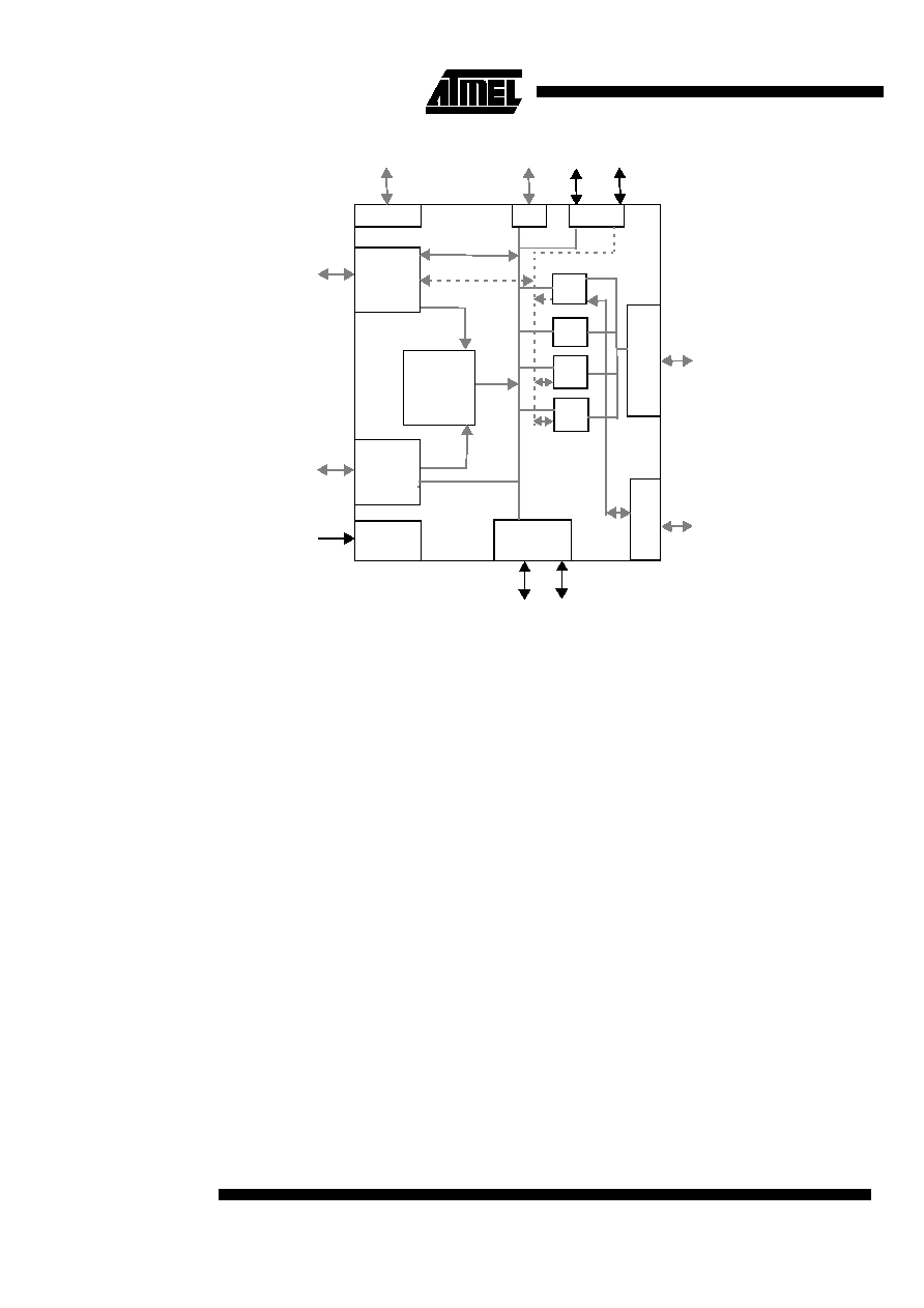
Block Diagram
Memory Interface
The RAM interface provides a 16-bit data bus and 16-bit address bus. Four chip select
lines allow to address four different memory partitions (banks). This partitioning into dif-
ferent banks is done using 4 internal address boundary registers. These are 8 bit wide
and provide a minimum page size of 1024 words. The memory interface can be pro-
grammed to use 0 to 7 wait states.
GPIO Interface
The general purpose I/O (GPIO Interface) provides up to 24 bidirectional signal lines.
The direction (input or output) of each GPIO line can be set individually via register.
Data to/from the GPIO lines is written/read via the GPIO data register. The GPIO pro-
vides 8 dedicated I/O lines, the remaining 16 lines of the port are shared with the ADC
address and host data bus. These GPIO lines are available when the corresponding unit
(e.g. the host data bus) of the T7906Eis not being used (disabled).
UART interface
Two independent UARTs are included in the T7906E as well. One UART uses dedi-
cated I/O lines whereas the second UART is sharing its pins with the GPIO port. The
transmit rate of the UARTs in bps can be programmed via a 12-bit wide register with a
maximum bit rate of about 780 kbit/s. The UARTs can optionally use hardware hand-
shake (rts/cts).
Host Interface
Although the T7906E is primarily designed to be remotely controlled, it can nevertheless
be programmed and controlled by a local host if required. For that purpose a host inter-
face provides 8 multiplexed data and address lines.
Timers / Event Counter
Two 32-bit on-chip timers are available on the T7906E. Each timer provides a 32 bit
counter and a 32 bit reload register. The two timers can be operated independently or
JTAG
UART
GPIO
Link
Interface
Host
Interface
system
util.
system
util.
Internal
Controller
Timer
Cont
rol B
u
s
Dat
a
B
u
s
ADC
I/F
ADC
I/F
ADC
I/F
ADC
I/F
DAC
I/F
RAM
I/F
FIFO
I/F
Internal
bus
control
& data control
address/command
bus
Internal control
data bus
transmit/receive
data bus
28
16
2
2
12
4
8
5
2
2