
Rev. C ≠ 3-Dec-01
1
Features
∑
80C52 Compatible
≠ 8051 pin and instruction compatible
≠ Four 8-bit I/O ports + 2 I/O I2C Interface pins
≠ Three 16-bit timer/counters
≠ 256 bytes scratch pad RAM
≠ 10 Interrupt sources with 4 priority levels
≠ Dual Data Pointer
∑
Variable length MOVX for slow RAM/peripherals
∑
ISP (In System Programming) using standard V
CC
power supply.
∑
Boot ROM contains low level FLASH programming routines and a default serial loader
∑
High-Speed Architecture
≠ 40 MHz in standard mode
≠ 20 MHz in X2 mode (6 clocks/machine cycle)
∑
32-Kbytes on-chip FLASH program / data Memory
≠ Byte and page (128 bytes) erase and write
≠ 10k write cycles
≠ On-chip 1024 bytes expanded RAM (XRAM)
≠ Software selectable size (0, 256, 512, 768, 1024 bytes)
≠ 256 bytes selected at reset for T87C51RB2/RC2 compatibility
∑
Keyboard interrupt interface on port P1
∑
400-Kbits/s Multimaster I
2
C Interface
∑
SPI Interface (Master / Slave Mode)
∑
Sub clock 32kHz crystal oscillator
∑
8-bit clock prescaler
∑
Improved X2 mode with independant selection for CPU and each peripheral
∑
Programmable Counter Array 5 Channels with:
≠
High Speed Output,
≠
Compare / Capture,
≠
Pulse Width Modulator,
≠
Watchdog Timer Capabilities
∑
Asynchronous port reset
∑
Full duplex Enhanced UART
∑
Dedicated Baud Rate Generator for UART
∑
Low EMI (inhibit ALE)
∑
Hardware Watchdog Timer (One-time enabled with Reset-Out)
∑
Power control modes:
≠ Idle Mode.
≠ Power-down mode.
≠ Power-Off Flag.
∑
Power supply: 4.5V to 5.5V or 2.7V to 3.6V
∑
Temperature ranges: Commercial (0 to +70
∞
C) and industrial (-40
∞
C to +85
∞
C).
∑
Packages: PLC44, VQFP44
Description
T89C51IC2 is a high performance FLASH version of the 80C51 8-bit microcontrollers.
It contains a 32-Kbytes Flash memory block for program and data.
The 32-Kbytes FLASH memory can be programmed either in parallel mode or in serial
mode with the ISP capability or with software. The programming voltage is internally
generated from the standard V
CC
pin.
The T89C51IC2 retains all features of the 80C52 with 256 bytes of internal RAM, a 7-
source 4-level interrupt controller and three timer/counters.
8-bit
Microcontroller
with Flash and
I
2
C Interface
T89C51IC2
Summary
2
T89C51IC2
Rev. C ≠ 3-Dec-01
In addition, the T89C51IC2 has a 32kHz Subsidiary clock Oscillator, a Programmable
Counter Array, an XRAM of 1024 byte, a Hardware Watchdog Timer, a Keyboard Inter-
face, a I2C Interface, a SPI Interface, a more versatile serial channel that facilitates
multiprocessor communication (EUART) and a speed improvement mechanism (X2
mode).
The fully static design of the T89C51IC2 allows to reduce system power consumption by
bringing the clock frequency down to any value, even DC, without loss of data.
The T89C51IC2 has 2 software-selectable modes of reduced activity and 8 bit clock
prescaler for further reduction in power consumption. In the Idle mode the CPU is frozen
while the peripherals and the interrupt system are still operating. In the power-down
mode the RAM is saved and all other functions are inoperative.
The added features of the T89C51IC2 make it more powerful for applications that need
pulse width modulation, high speed I/O and counting capabilities such as alarms, motor
control, corded phones, smart card readers.
Table 1. Memory Size
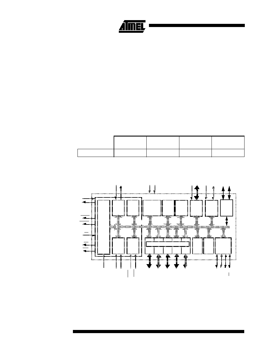
Block Diagram
PLCC44
VQFP44 1.4
Flash (bytes)
XRAM (bytes)
TOTAL RAM
(bytes)
I/O
T89C51IC2
32k
1024
1280
34
Timer 0
INT
RAM
256x8
T0
T1
Rx
D
Tx
D
WR
RD
EA
PSEN
ALE/
XTAL2
XTAL1
EUART
CPU
Timer 1
IN
T
1
Ctrl
IN
T
0
( 2)
( 2)
C51
CORE
(2) (2)
(2) ( 2)
Port 0
P0
Port 1 Port 2 Port 3
Parallel I/O Ports & Ext. Bus
P1
P2
P3
XRAM
1Kx8
IB-bus
PCA
RE
S
E
T
PROG
Watch
Dog
PC
A
EC
I
Vs
s
V
CC
(2)
(2)
( 1)
(1): Alternate function of Port 1
(2): Alternate function of Port 3
(1)
Timer2
T2
E
X
T2
(1)
(1)
Port I2
PI
2
F las h
32K x8 or
16K x8
Key
B oard
ROM
2Kx8
Boot
+
BRG
SPI
MI
S
O
MO
S
I
SC
K
(1) (1) (1)
SS
( 1)
I
2
C
SD
A
SC
L

3
T89C51IC2
Rev. C ≠ 3-Dec-01
SFR Mapping
The Special Function Registers (SFRs) of the T89C51IC2 fall into the following
categories:
∑
C51 core registers: ACC, B, DPH, DPL, PSW, SP
∑
I/O port registers: P0, P1, P2, P3, PI2
∑
Timer registers: T2CON, T2MOD, TCON, TH0, TH1, TH2, TMOD, TL0, TL1, TL2,
RCAP2L, RCAP2H
∑
Serial I/O port registers: SADDR, SADEN, SBUF, SCON
∑
PCA (Programmable Counter Array) registers: CCON, CCAPMx, CL, CH, CCAPxH,
CCAPxL (x: 0 to 4)
∑
Power and clock control registers: PCON
∑
Hardware Watchdog Timer registers: WDTRST, WDTPRG
∑
Interrupt system registers: IE0, IPL0, IPH0, IE1, IPL1, IPH1
∑
Keyboard Interface registers: KBE, KBF, KBLS
∑
SPI registers: SPCON, SPSTR, SPDAT
∑
I2C Interface registers: SSCON, SSCS, SSDAT, SSADR
∑
BRG (Baud Rate Generator) registers: BRL, BDRCON
∑
Flash register: FCON
∑
Clock Prescaler register: CKRL
∑
32Khz Sub Clock Oscillator registers: CKSEL, OSSCON
∑
Others: AUXR, AUXR1, CKCON0, CKCON1

4
T89C51IC2
Rev. C ≠ 3-Dec-01
Table 2. SFR mapping
Table below shows all SFRs with their address and their reset value.
Bit
addressable
Non Bit addressable
0/8
1/9
2/A
3/B
4/C
5/D
6/E
7/F
F8h
CH
0000 0000
CCAP0H
XXXX XXXX
CCAP1H
XXXX XXXX
CCAPL2H
XXXX XXXX
CCAPL3H
XXXX XXXX
CCAPL4H
XXXX XXXX
FFh
F0h
B
0000 0000
F7h
E8h
CL
0000 0000
CCAP0L
XXXX XXXX
CCAP1L
XXXX XXXX
CCAPL2L
XXXX XXXX
CCAPL3L
XXXX XXXX
CCAPL4L
XXXX XXXX
EFh
E0h
ACC
0000 0000
E7h
D8h
CCON
00X0 0000
CMOD
00XX X000
CCAPM0
X000 0000
CCAPM1
X000 0000
CCAPM2
X000 0000
CCAPM3
X000 0000
CCAPM4
X000 0000
DFh
D0h
PSW
0000 0000
FCON (1)
XXXX 0000
D7h
C8h
T2CON
0000 0000
T2MOD
XXXX XX00
RCAP2L
0000 0000
RCAP2H
0000 0000
TL2
0000 0000
TH2
0000 0000
CFh
C0h
PI2 bit
addressable
XXXX XX11
SPCON
0001 0100
SPSTA
0000 0000
SPDAT
XXXX XXXX
C7h
B8h
IPL0
X000 000
SADEN
0000 0000
BFh
B0h
P3
1111 1111
IE1
XXXX X000
IPL1
XXXX X000
IPH1
XXXX X111
IPH0
X000 0000
B7h
A8h
IE0
0000 0000
SADDR
0000 0000
CKCON1
XXXX XXX0
AFh
A0h
P2
1111 1111
AUXR1
XXXX X0X0
WDTRST
XXXX XXXX
WDTPRG
XXXX X000
A7h
98h
SCON
0000 0000
SBUF
XXXX XXXX
BRL
0000 0000
BDRCON
XXX0 0000
KBLS
0000 0000
KBE
0000 0000
KBF
0000 0000
9Fh
90h
P1
1111 1111
SSCON
0000 0000
SSCS
1111 1000
SSDAT
1111 1111
SSADR
1111 1110
CKRL
1111 1111
97h
88h
TCON
0000 0000
TMOD
0000 0000
TL0
0000 0000
TL1
0000 0000
TH0
0000 0000
TH1
0000 0000
AUXR
XX0X 0000
CKCON0
0000 0000
8Fh
80h
P0
1111 1111
SP
0000 0111
DPL
0000 0000
DPH
0000 0000
CKSEL
XXXX XXX0
OSSCON
XXXX X001
PCON
00X1 0000
87h
0/8
1/9
2/A
3/B
4/C
5/D
6/E
7/F
reserved
(1) FCON access is reserved for the FLASH API and ISP software.
5
T89C51IC2
Rev. C ≠ 3-Dec-01
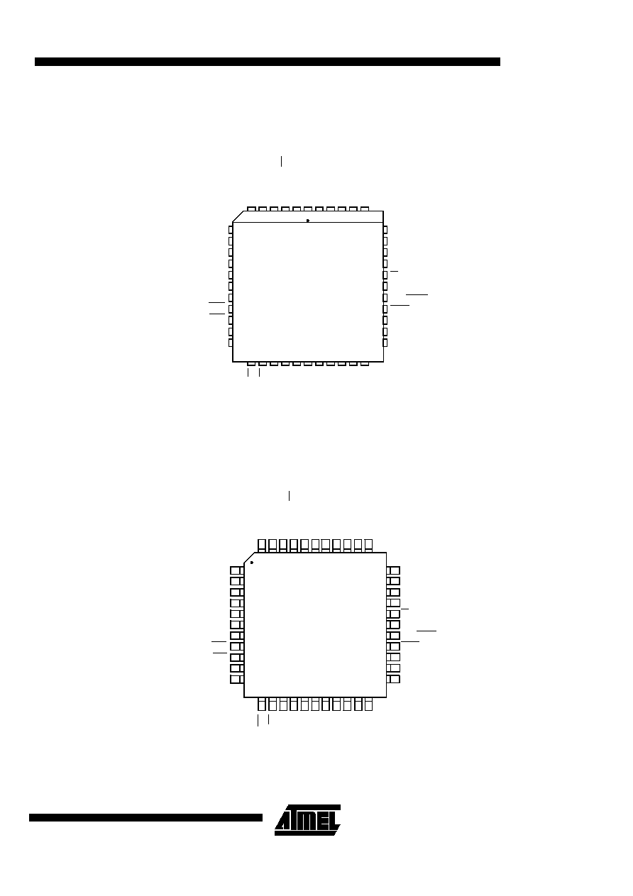
Pin Configurations
18 19
23
22
21
20
26
25
24
27 28
5
4
3
2
1
6
44 43 42 41 40
P
1
.4/C
E
X
1
P
1
.0/T
2/
X
T
A
L
B
1
P
1
.1/T
2E
X
/
S
S
P
1
.3/C
E
X
0
P
1
.2/E
CI
XT
A
L
B2
VC
C
P
0
.0/A
D0
P
0
.2/A
D2
P
0
.1/A
D1
P0.4/AD4
P0.6/AD6
P0.5/AD5
P0.7/AD7
ALE/PROG
PSEN
EA
PI2.0/SCL
P2.7/A15
P2.5/A13
P2.6/A14
P
3
.6/W
R
P
3
.7/RD
XT
A
L
2
XT
A
L
1
VS
S
P
2
.0/A
8
P
2
.1/A
9
P
2
.2/A
10
P
2
.3/A
1
1
P
2
.4/A
12
P1.5/CEX2/MISO
P1.6/CEX3/SCK
P1.7/CEx4/MOSI
RST
P3.0/RxD
PI2.1/SDA
P3.1/TxD
P3.2/INT0
P3.3/INT1
P3.4/T0
P3.5/T1
P
0
.3
/A
D3
NIC
*
7
8
9
10
11
12
13
14
15
16
17
39
38
37
36
35
34
33
32
31
30
29
PLCC44
43 42 41 40 39
44
38 37 36 35 34
P1
.
4
/
C
E
X
1
P1
.
0
/
T
2
/
XT
AL
B
1
P1
.
1
/
T
2
E
X
/
SS
P1
.
3
/
C
E
X
0
P1
.
2
/
E
C
I
XT
A
L
B2
VC
C
P0
.
0
/
A
D
0
P0
.
2
/
A
D
2
P0
.
3
/
A
D
3
P0
.
1
/
A
D
1
P0.4/AD4
P0.6/AD6
P0.5/AD5
P0.7/AD7
ALE/PROG
PSEN
EA
PI2.0/SCL
P2.7/A15
P2.5/A13
P2.6/A14
P1.5/CEX2/MISO
P1.6/CEX3/SCK
P1.7/CEX4/MOSI
RST
P3.0/RxD
PI2.1/SDA
P3.1/TxD
P3.2/INT0
P3.3/INT1
P3.4/T0
P3.5/T1
P
3
.6
/W
R
P3
.
7
/
R
D
XT
A
L
2
XT
A
L
1
VS
S
P
2
.0
/A
8
P2
.
1
/
A
9
P
2
.2
/A
1
0
P
2
.3
/A
1
1
P
2
.4
/A
1
2
NI
C*
12 13
17
16
15
14
20
19
18
21 22
33
32
31
30
29
28
27
26
25
24
23
VQFP44 1.4
1
2
3
4
5
6
7
8
9
10
11