Rev. 4194B≠AUTO≠12/04
1
Features
∑
Fully Compliant to VAN Specification ISO/11519.3
∑
Handles All Specified Module Types
∑
Handles All Specified Message Types
∑
Handles Retransmission of Frames on Contention and Errors
∑
3 Separate Line Inputs with Automatic Diagnosis and Selection
∑
1 Mbit/s Maximum Transfer Rate
∑
Normal or Pulsed (Optical and Radio Mode) Coding
∑
Intel
Æ
, NEC
Æ
, Texas Instruments
Æ
and Motorola
Æ
Compatible 8-bit Microprocessor
Interface
∑
Multiplexed Address and Data Bus
∑
Idle and Sleep Modes
∑
128 Bytes of General-purpose RAM
∑
DMA Capabilities for Message Handling
∑
14 Identifier Registers with All Bits Individually Maskable
∑
6-source Maskable Interrupt Including an Interrupt-on-reset to Detect Glitches on the
Reset Pin
∑
Integrated Crystal or Resonator Oscillator with Internal Baud Rate Generator and
Buffered Clock Output
∑
Single +5V Power Supply
∑
0.5 mm CMOS Technology
∑
SOP 24 Packaging
Description
Cost optimization in car manufacturing is of extreme importance today. Solutions to
this problem often implies the use of more advanced and intelligent electronic circuits.
The TSS461E is a circuit which allows the transfer of all the status information needed
in a car or truck over a single low-cost wire pair, thereby, minimizing the electrical wire
usage.
It can be used to interconnect powerful functions (ABS, dashboard, power train con-
trol) and to control and interface car body electronics (lights, wipers, power window,
etc.).
The TSS461E is fully compliant with the ISO standard 11519-3. This standard sup-
ports a wide range of applications such as low-cost remote control switches, typically
used for lamp control; complex, highly-autonomous, distributed systems like engine
controls, which require fast and secure data transfers.
The TSS461E is a microprocessor-interfaced line controller for mid-to-high complexity
bus-masters and listeners like injection/ignition control calculators, dashboard control-
lers and car stereo or mobile telephone CPUs.
The microprocessor interface consists of a 256-bytes of RAM and the register area is
divided into 11 control registers, 14 channel register sets and 128 bytes of general
purpose RAM, used as a message storage area, and a 6-source maskable interrupt.
The circuit operates in RAM using DMA techniques, controlled by the channel and
control registers. This allows virtually any microprocessor to interface with ease to the
TSS461E, and to use the free RAM as a scratch pad.
Messages are encoded in enhanced Manchester code, and an optional pulsed code
for use with an optical or radio link, at a maximum bit rate of 1 Mbit/s. The TSS461E
analyzes the messages received or transmitted according to 6 different criteria includ-
ing some higher level checks.
In addition, the bus interface has three separate inputs with automatic source diagno-
sis and selection, allowing for multibus listening or the automatic selection of the most
reliable source at any time if several line receivers are connected to the same bus.
VAN Data Link
Controller
TSS461E

5
TSS461E
4194B≠AUTO≠12/04
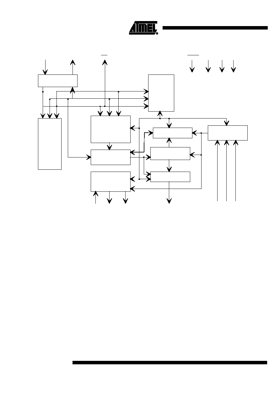
Operation
The TSS461E is a microprocessor-controlled line controller for the VAN bus. It can inter-
face to virtually any microprocessor, but the I/O signals of the circuit have been
optimized for use with the TSC51/TSC251 series of microcontrollers.
It features a multiplexed address and data bus, controlled by an address strobe pin ALE
and separated read RD and write WR command pins. The address is latched on the fall-
ing edge of ALE.
The circuit also features one single interrupt pin. This pin can be treated as level or edge
sensitive, For example, if there is a pending interrupt inside the circuit when another
interrupt is reset, the INT pin will emit a high pulse with the same pulse width as the
internal write strobe (typically 20 ns).
Figure 2. Typical Application
Remaining Pins
TSS461E
Microcontroller
Series
P3.6/WR
P3.7/RD
ALE
P0.7
P0.6
P0.5
P0.4
P0.3
P0.2
P0.1
P0.0
WR
RD
ALE
AD7
AD6
AD5
AD4
AD3
AD2
AD1
AD0
XTAL1
XTAL2
TXD
RXD0
RXD1
RXD2
CS
VAN
DLC
INT CKOUT RESET
RESET XTAL1 INT
V
CC
33 pF
C1
GND
GND
+
-
+
-
+
-
V
REF
DATA
DATA
Differential
D
A
T
A
DA
T
A
VAN Bus
VAN Line Driver
& Receivers
General I/O