 | –≠–ª–µ–∫—Ç—Ä–æ–Ω–Ω—ã–π –∫–æ–º–ø–æ–Ω–µ–Ω—Ç: U211B-x | –°–∫–∞—á–∞—Ç—å:  PDF PDF  ZIP ZIP |
U211B
Rev. A4, 03-Aug-01
1 (21)
Phase-Control IC ≠ Tacho Applications/Overload Limitation
Description
The integrated circuit U211B is designed as a phase-con-
trol circuit in bipolar technology with an internal
frequency-voltage converter. Furthermore, it has an inter-
nal control amplifier which means it can be used for
speed-regulated motor applications.
It has an integrated load limitation, tacho monitoring and
soft-start functions, etc. to realize sophisticated motor
control systems.
Features
D Internal frequency-to-voltage converter
D Externally-controlled integrated amplifier
D Overload limitation with a "fold back" characteristic
D Optimized soft-start function
D Tacho monitoring for shorted and open loop
D Automatic retriggering switchable
D Triggering pulse typ. 155 mA
D Voltage and current synchronization
D Internal supply-voltage monitoring
D Temperature reference source
D Current requirement
3 mA
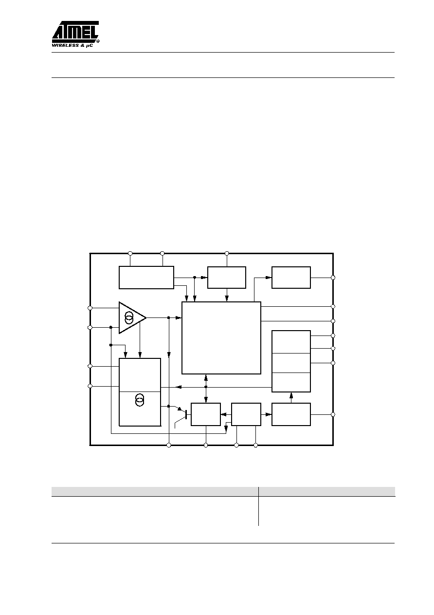
Block Diagram
Control
amplifier
Load limitation
speed / time
controlled
Voltage
monitoring
Supply
voltage
limitation
Reference
voltage
Output
pulse
Pulse-blocking
tacho
monitoring
Frequency-
to-voltage
converter
= f (V
12
)
Phase
-
control unit
Soft start
11(10)
12(11)
13(12)
9(8)
8(7)
18*)
Voltage / current
detector
Automatic
retriggering
17(16)
1(1)
4(4)
5*)
≠V
S
GND
+
≠
≠V
Ref
6(5)
7(6)
3(3)
2(2)
16(15)
10(9)
14(13)
15(14)
ˆ
controlled
current sink
Figure 1. Block diagram (Pins in brackets refer to SO16)
*) Pins 5 and 18 connected internally
Order Information
Extended Type Number
Package
Remarks
U211B-x
DIP18
Tube
U211B-xFP
SO16
Tube
U211B-xFPG3
SO16
Taped and reeled
U21
1B
Rev
. A4,
03-Aug-01
2 (21)
R
3
220 k
W
R
4
470 k
W
R
2
≠V
S
3.3 nF
1 M
W
GND
C
1
22
25 V
C
11
2.2
R
12
180
W
M
R
1
18 k
W
1N4007
D
1
2 W
TIC
226
R
8
33 m
W
1 W
R
11
2 M
W
100 k
W
R
6
C
6
100 nF
10 /16V
C
7
C
8
220 nF
22 k
W
R
7
C
3
2.2
16 V
C
5
1 nF
R
5
1 k
W
Speed sensor
C
4
220 nF
L
N
1 k
W
R
10
R
9
1 M
W
4.7 /16V
C
9
R
19
100 k
W
C
10
2.2 /16V
R
31
100 k
W
R
14
56 k
W
R
13
47 k
W
V
M
=
230 V ~
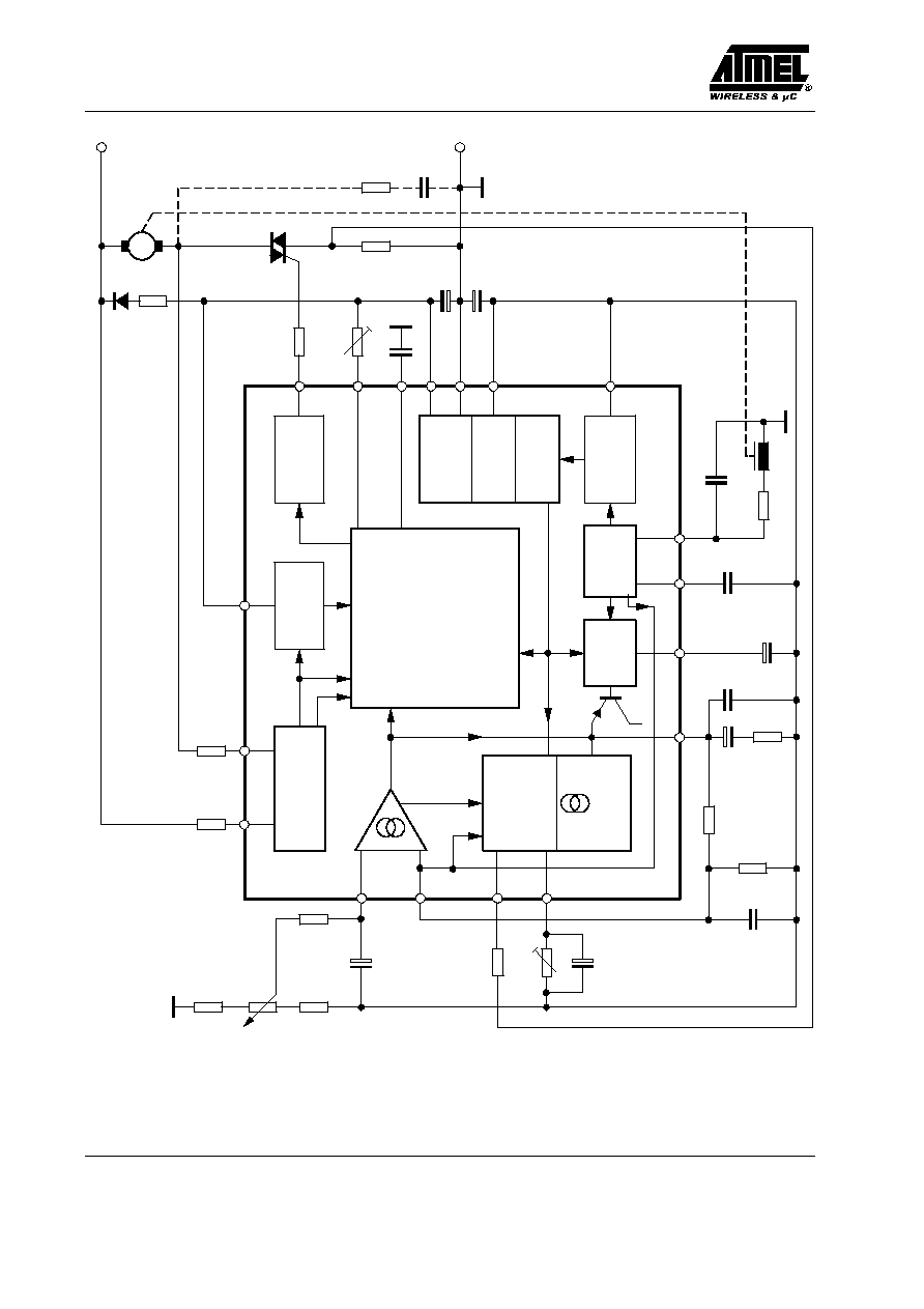
Control
amplifier
Load limitation
speed / time
controlled
Voltage
monitoring
Supply
voltage
limitation
Reference
voltage
Output
pulse
Pulse blocking
tacho
monitoring
Frequency-
to-voltage
converter
Phase-
control unit
Soft start
15
14
11
10
12
13
9
8
7
3
2
16
18
Voltage / current
detector
Automatic
retriggering
17
1
6
4
5
= f (V
12
)
+
≠
C
2
Set speed
voltage
Actual speed
voltage
mF
mF
mF
mF
mF
mF
ˆ
controlled
current sink
≠V
Ref
Figure
2. Speed control, automatic retriggering, load limiting, soft start
U211B
Rev. A4, 03-Aug-01
3 (21)
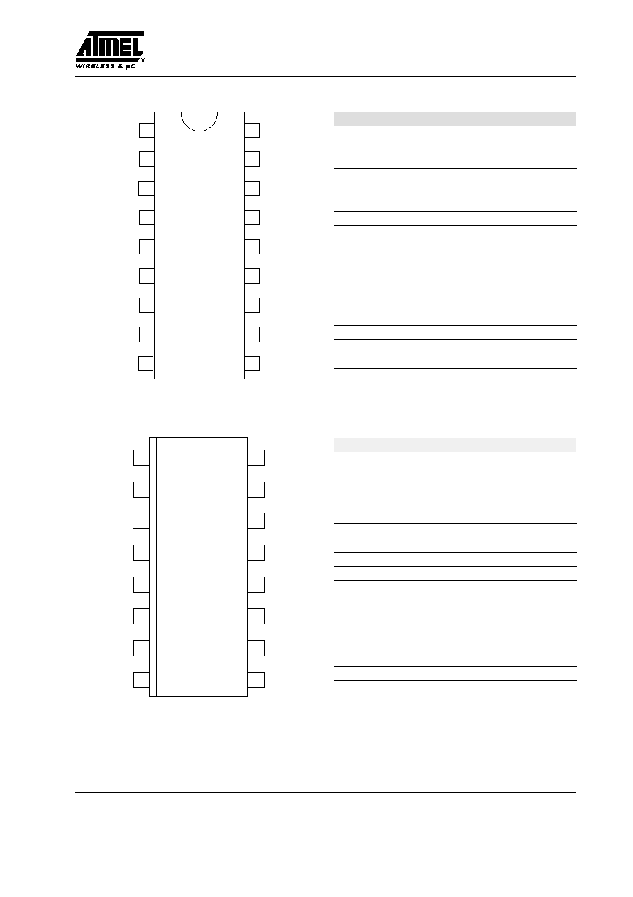
Pin Description
1
2
3
4
5
6
7
8
10
9
18
17
16
14
15
13
12
11
V
S
Output
Retr
V
RP
C
P
F/V
I
sync
GND
V
Ref
OVL
I
sense
C
soft
CTR/OPO
OP+
PB/TM
V
sync
C
RV
OP≠
U211B
Figure 3. Pinning DIP18
Pin
Symbol
Function
1
I
sync
Current synchronization
2
GND
Ground
3
V
S
Supply voltage
4
Output
Trigger pulse output
5
Retr
Retrigger programming
6
V
RP
Ramp current adjust
7
C
P
Ramp voltage
8
F/V
Frequency-voltage converter
9
C
RV
Charge pump
10
OP≠
OP inverting input
11
OP+
OP non-inverting input
12
CTR/OPO Control input / OP output
13
C
soft
Soft start
14
I
sense
Load-current sensing
15
OVL
Overload adjust
16
V
ref
Reference voltage
17
V
sync
Voltage synchronization
18
PB/TM
Pulse blocking /
tacho monitoring
V
S
Output
V
RP
C
P
F/V
C
RV
I
sync
GND
1
2
3
4
5
6
7
8
16
15
14
13
12
11
10
9
OVL
I
sense
C
soft
CTR/OPO
OP+
OP≠
V
sync
V
Ref
U211B
Figure 4. Pinning SO16
Pin
Symbol
Function
1
I
sync
Current synchronization
2
GND
Ground
3
V
S
Supply voltage
4
Output
Trigger pulse output
5
V
RP
Ramp current adjust
6
C
P
Ramp voltage
7
F/V
Frequency-voltage converter
8
C
RV
Charge pump
9
OP≠
OP inverting input
10
OP+
OP non-inverting input
11
CTR/OPO Control input / OP output
12
C
soft
Soft start
13
I
sense
Load-current sensing
14
OVL
Overload adjust
15
V
ref
Reference voltage
16
V
sync
Voltage synchronization
U211B
Rev. A4, 03-Aug-01
4 (21)
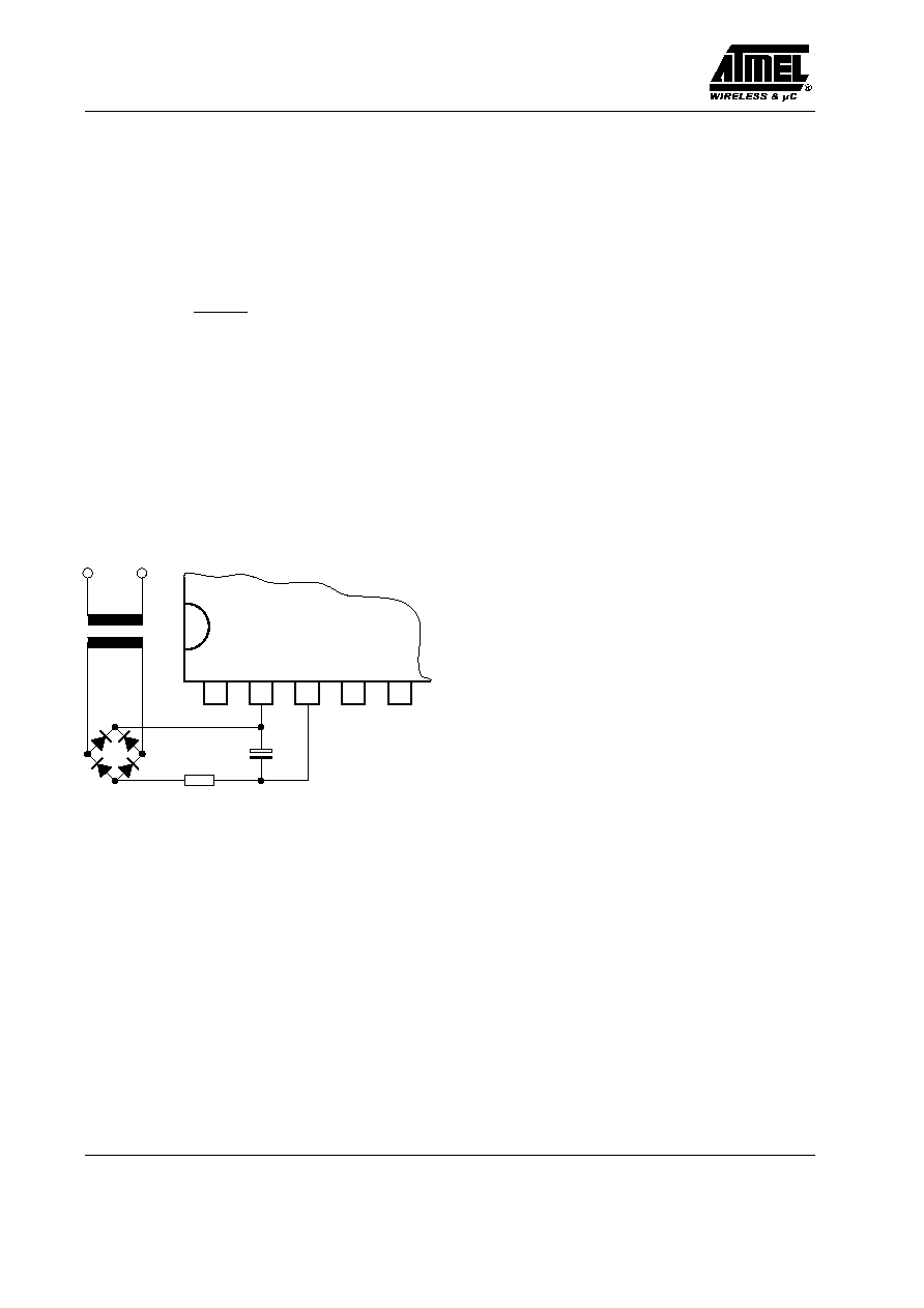
Description
Mains Supply
The U211B is fitted with voltage limiting and can
therefore be supplied directly from the mains. The supply
voltage between Pin 2 (+ pol/
) and Pin 3 builds up
across D
1
and R
1
and is smoothed by C
1
. The value of the
series resistance can be approximated using:
R
1
+
V
M
≠ V
S
2 I
S
Further information regarding the design of the mains
supply can be found in the design hints. The reference
voltage source on Pin 16 of typ. ≠8.9 V is derived from
the supply voltage and is used for regulation.
Operation using an externally stabilized DC voltage is not
recommended.
If the supply cannot be taken directly from the mains
because the power dissipation in R
1
would be too large,
then the circuit shown in figure 5 should be used.
1
2
3
4
5
C
1
R
1
24 V~
~
Figure 5. Supply voltage for high current requirements
Phase Control
The phase angle of the trigger pulse is derived by compar-
ing the ramp voltage (which is mains synchronized by the
voltage detector) with the set value on the control input
Pin 12. The slope of the ramp is determined by C
2
and its
charging current. The charging current can be varied
using R
2
on Pin 6. The maximum phase angle
a
max
can
also be adjusted using R
2
.
When the potential on Pin 7 reaches the nominal value
predetermined at Pin 12, then a trigger pulse is generated
whose width t
p
is determined by the value of C
2
(the value
of C
2
and hence the pulse width can be evaluated by
assuming 8
ms/nF). At the same time, a latch is set, so that
as long as the automatic retriggering has not been
activated, no more pulses can be generated in that half
cycle.
The current sensor on Pin 1 ensures that, for operations
with inductive loads, no pulse will be generated in a new
half cycle as long as a current from the previous half cycle
is still flowing in the opposite direction to the supply
voltage at that instant. This makes sure that "gaps" in the
load current are prevented.
The control signal on Pin 12 can be in the range 0 V to
≠7 V (reference point Pin 2).
If V
12
=
≠7 V, the phase angle is at maximum
=
a
max,
i.e.,
the current flow angle is a minimum. The phase angle
a
min
is minimum when V
12
= V
2
.
Voltage Monitoring
As the voltage is built up, uncontrolled output pulses are
avoided by internal voltage surveillance. At the same
time, all latches in the circuit (phase control, load limit
regulation, soft start) are reset and the soft-start capacitor
is short circuited. Used with a switching hysteresis of
300 mV, this system guarantees defined start-up behavior
each time the supply voltage is switched on or after short
interruptions of the mains supply.
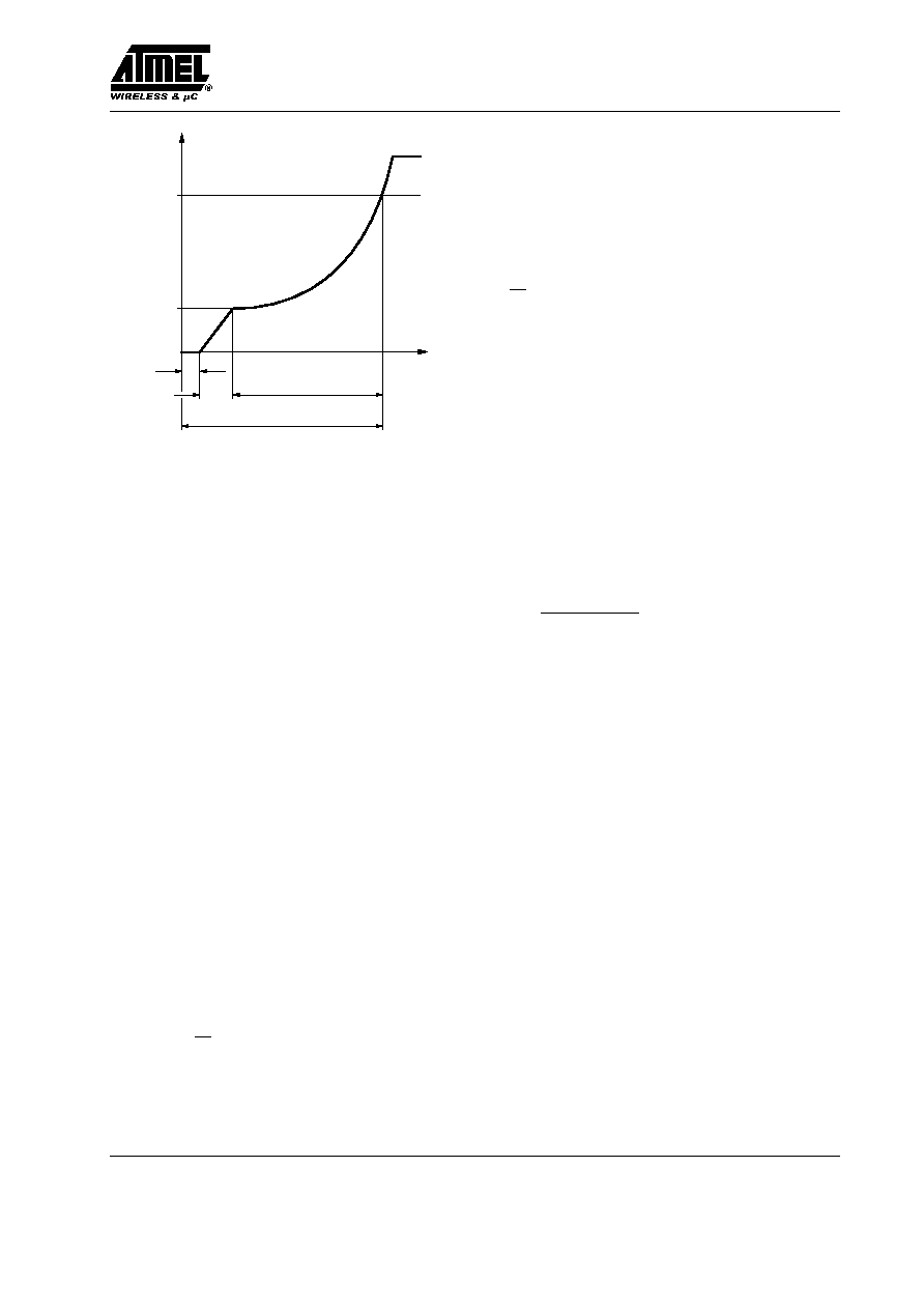
Soft Start
As soon as the supply voltage builds up (t
1
), the integrated
soft start is initiated. Figure 6 shows the behaviour of the
voltage across the soft-start capacitor which is identical
with the voltage on the phase-control input on Pin 12.
This behavior guarantees a gentle start-up for the motor
and automatically ensures the optimum run-up time.
U211B
Rev. A4, 03-Aug-01
5 (21)
V
C3
t
V
12
V
0
t
1
t
tot
t
2
t
3
Figure 6. Soft start
t
1
= build-up of supply voltage
t
2
= charging of C
3
to starting voltage
t
1
+ t
2
= dead time
t
3
= run-up time
t
tot
= total start-up time to required speed
C
3
is first charged up to the starting voltage V
0
with a
current of typically 45
mA (t
2
). By then reducing the
charging current to approx. 4
mA, the slope of the
charging function is substantially reduced so that the
rotational speed of the motor only slowly increases. The
charging current then increases as the voltage across C
3
increases, resulting in a progressively rising charging
function which accelerates the motor more and more with
increasing rotational speed. The charging function
determines the acceleration up to the set-point. The
charging current can have a maximum value of 55
mA.
Frequency-to-Voltage Converter
The internal frequency-to-voltage converter (f/V-
converter) generates a DC signal on Pin 10 which is
proportional to the rotational speed using an AC signal
from a tacho generator or a light beam whose frequency
is in turn dependent on the rotational speed. The high-
impedance input Pin 8 compares the tacho voltage to a
switch-on threshold of typ. ≠100 mV. The switch-off
threshold is given with ≠50 mV. The hysteresis
guarantees very reliable operation even when relatively
simple tacho generators are used. The tacho frequency is
given by:
f
+ n
60
p (Hz)
where:
n = revolutions per minute
p = number of pulses per revolution
The converter is based on the charge pumping principle.
With each negative half wave of the input signal, a
quantity of charge determined by C
5
is internally
amplified and then integrated by C
6
at the converter
output on Pin 10. The conversion constant is determined
by C
5
, its charge transfer voltage of V
ch
, R
6
(Pin 10) and
the internally adjusted charge transfer gain.
G
i
I
10
I
9
+ 8.3
k = G
i
C
5
R
6
V
ch
The analog output voltage is given by
V
O
= k
f
The values of C
5
and C
6
must be such that for the highest
possible input frequency, the maximum output voltage
V
O
does not exceed 6 V. While C
5
is charging up, the R
i
on Pin 9 is approximately 6.7 k
W. To obtain good
linearity of the f/V converter, the time constant resulting
from R
i
and C
5
should be considerably less (1/5) than the
time span of the negative half-cycle for the highest
possible input frequency. The amount of remaining ripple
on the output voltage on Pin 10 is dependent on C
5
, C
6
and
the internal charge amplification.
V
O
=
G
i
V
ch
C
5
C
6
The ripple
V
o
can be reduced by using larger values of
C
6
. However, the increasing speed will then also be
reduced.
The value of this capacitor should be chosen to fit the
particular control loop where it is going to be used.
Pulse Blocking
The output of pulses can be blocked by using Pin 18
(standby operation) and the system reset via the voltage
monitor if V
18
≠1.25 V. After cycling through the
switching point hysteresis, the output is released when
V
18
≠1.5 V followed by a soft start such as that after
turn-on.
Monitoring of the rotation can be carried out by
connecting an RC network to Pin 18. In the event of a
short or open circuit, the triac triggering pulses are cut off
by the time delay which is determined by R and C. The
capacitor C is discharged via an internal resistance
R
i
= 2 k
W with each charge transfer process of the f/V
converter. If there are no more charge transfer processes,
C is charged up via R until the switch-off threshold is
exceeded and the triac triggering pulses are cut off. For
operation without trigger pulse blocking or monitoring of
the rotation, Pins 18 and 16 must be connected together.