U2403B
Rev. A4, 12-Jan-01
1 (12)
Charge Timer
Description
The U2403B is a monolithic, integrated bipolar circuit
which can be used in applications for time-controlled,
constant-current charge. Selection of charge current
versus timing is carried out by using the external circuit
at Pins 2, 3 and 4. For high current requirement, an
external transistor is recommended in series with the
battery. To protect the IC against high power loss
(typically > 140
∞
C), the oscillator is shut down when the
reference voltage is switched off (0 V). The latter also
takes place when there is a saturation caused by collector
voltage at Pin 1. When the overtemperature has
disappeared and the collector voltage at Pin 1 has
exceeded the supply voltage (V
1
> V
S
), charge time
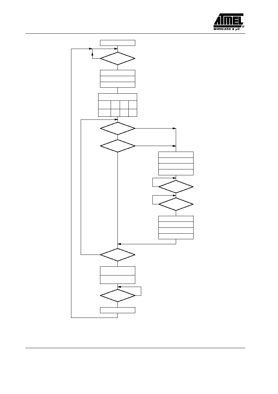
operation continues (see flow chart in figure 4).
Features
D Easy-to-run autonomous dual rate charger
D Constant charge current
D 3 h ≠ 24 h charge time programmable
D Low-cost DC regulator
D Overtemperature protection
D Charge-mode indication
D Operation starts at the moment of battery insertion
D Fast charge-time test mode
Applications
D Cordless telephones
D Low-cost battery-charge timer
D Entertainment
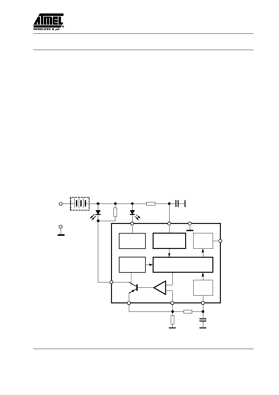
Block Diagram
Power supply
V
S
= 3.5 to 12 V
Charge mode
indicator
Test
mode
RC
oscillator
Ì max
140
∞
C
Ì
8
6
5
4
3
2
1
7
Power
supply
AC/DC
Battery
inserted
R
4
LED
GND
V
S
S
TM
V
1
Shunt
Sense
Osc
R
3
C
4
+
≠
Timer and control logic
V
Ref
= 1.5 V/ 0.1 V/ 0 V
V
Ref
R
1
C
1
R
5
LED
2
LED
1
Charge
Ready
Figure 1. Block diagram with external circuit

U2403B
Rev. A4, 12-Jan-01
2 (12)
Ordering Information
Extended Type Number
Package
Remarks
U2403B-x
DIP8
Tube
U2403B-xFP
SO8
Tube
U2403B-xFPG3
SO8
Taped and reeled
Pin Description
1
2
3
4
8
7
6
5
V
1
V
2
Sense
Osc
LED
U2403B
V
S
S
TM
Figure 2. Pinning
Pin
Symbol
Function
1
V
1
Collector terminal
2
V
2
Shunt emitter terminal
3
V
3
Amplifier sense input
4
Osc
Oscillator input
5
S
TM
Test mode switch
6
V
S
Supply voltage
7
GND
Reference point, GND
8
LED
Charge mode indicator
Pin 1, Collector Voltage V
1
Pin 1 is an open collector output. When V
1
3 V, the
charge cycle is switched off until it is above the supply
voltage, as shown in figure 6.
Pin 2, Shunt Emitter
The constant current source is supplied by the internal
operational amplifier. The voltage across R
3
is deter-
mined via the internal reference source.
I
ch
= V
3
/R
3
(V
3
= V
sense
)
Pin 3, Amplifier Sense Input (Inverted)
The voltage-regulated current source has a closed loop at
Pin 2, Pin 3, and resistor R
3
.
Pin 4, Oscillator Input R
4
, C
4
Selection of current charge versus timing is carried out by
using the external circuit at Pins 2, 3, and 4. Typical
values are given in charge characteristics (see table next
page).
Pin 5, Test-Mode Switch for Charging Time
The charging time, t
ch,
is given by the following equation.
t
ch
+ 1
f
osc
2
n
where:
f
osc
= oscillator frequency (see figure 3)
n
= frequency divider
= 26, if S
TM
open
= 17, if S
TM
= GND
= 8, if S
TM
= V
S
The first eight divider stages can be tested directly.
256 input tact signals at Pin 4 create one tact signal at
Pin 5.
1
2
3
256
Oscillator
Pulse
Test ≠ Mode
Pin 4
Pin 5
Figure 3. Quick test timer 1/3
Example
Assume a charge time of 6 h.
Select the values of R
4
and C
4
from the tables next page.
For example:
R
4
= 470 k
W
C
4
= 680 pF
There is a frequency of approximately 3100 Hz at Pin 4.
It is possible to test the charge time of 6 h by running
through the charge cycle for a very short time. By
connecting Pin 5 with GND, the test time is 42 s. By
connecting Pin 5 with Pin 1 (V
1
), the test time is reduced
to about 82.4 ms. R
5
is connected in parallel to the LED
2
and provides a protective bypass function for the LED
(see figure 1).
U2403B
Rev. A4, 12-Jan-01
3 (12)
Pin 6, Supply Voltage, V
S
V
S
[ 3.1 V power-on reset release (turn-on)
V
S
[ 2.9 V under-voltage reset
V
S
[ 13 V supply voltage limitation
Pin 7, Ground
Pin 8, Charge Mode Indicator
An open-collector output supplies constant current to
LED
1
after the active charge phase has been terminated.
Ì
max
controls the function temperature for the final stage
range. This is when the temperature is above 140
∞
C and
the charge function is therefore switched off.
Trickle Charge
The trickle charge starts after the charge has been termi-
nated. In this case, the internal reference voltage is
reduced from 1.5 V to approximately 0.1 V. This means
the charge current is decreased by the factor:
K = 1.5 V/ 0.1 V = 15.
Trickle current = I
ch
/ 15 + I
6
(supply current) + I
8
It is possible to reduce the trickle charge with resistor R
6,
as shown in figures 7 and 8.
Charge Characteristics
Charge Time
Test Time/ Test-Mode Switch S
TM
Oscillator Components
Frequency
Open
V
S
GND
R
4
(k
W)
C
4
(pF)
f
osc
(Hz)
3 h
41.2 ms
21 s
510
430
300
270
330
470
6213
4 h
54.9 ms
28 s
620
430
300
330
470
680
4660
5 h
68.6 ms
35 s
510
390
300
470
680
1000
3728
6 h
82.4 ms
42 s
620
470
360
470
680
1000
3105
7 h
96.1 ms
49 s
560
430
220
680
1000
2200
2663
8 h
109.8 ms
56 s
620
470
200
680
1000
2200
2330
9 h
123.6 ms
1 min 3 s
750
510
240
680
1000
2200
2071
10 h
137.3 ms
1 min 10 s
620
270
130
820
2200
4700
1864
12 h
164.8 ms
1 min 24 s
390
150
2200
4700
1553
16 h
219.7 ms
1 min 56 s
470
200
2200
4700
1165
U2403B
Rev. A4, 12-Jan-01
4 (12)
Battery
inserted
LED
2
"ON"
start
Test
Open
Divider
GND
Turn on V
S
> 3.5 V
V
3
= 1.5 V
V
S
2
26
2
17
2
8
Timer start
T
j
> T
max
no
V
1
< 3.0 V
yes
yes
LED
2
"OFF"
V
3
[0 V
Interrupt charging
Interrupt
V
1
> V
S
no
no
yes
LED
2
"ON"
Continuous charging
Continuous timing
End of
timing
Trickle charge mode
LED
2
"OFF"
LED
1
"ON"
Battery
removed
Undervoltage reset
no
no
yes
no
yes
no
yes
T
j
< T
max
V
3
= 0 V
V
3
= 100 mV
mode
Figure 4. Flow chart
U2403B
Rev. A4, 12-Jan-01
5 (12)
Absolute Maximum Ratings
Reference point Pin 7 (GND), unless otherwise specified.
Parameters
Symbol
Value
Unit
Supply current
Pin 6
t
100
ms
I
S
i
s
20
100
mA
mA
Currents
Pin 1
Pin 2
Pin 3
Pin 4
Pin 5
Pin 8
I
1
≠I
2
I
3
I
4
I
5
I
8
300
310
1
15
≠75 to +120
8
mA
mA
mA
mA
mA
mA
Voltages
Pins 1, 3, 5, 6 and 8
Pin 2
Pin 4
V
V
2
V
4
13.5
1.6
1.5
V
V
V
Junction temperature
T
j
150
∞
C
Ambient temperature
T
amb
≠10 to 85
∞
C
Storage temperature range
T
stg
≠50 to +150
∞
C
Thermal Resistance
Parameters
Symbol
Value
Unit
Junction ambient
DIP8
SO8 on PC-board
SO8 on ceramic
SO8 on ceramic with thermal compound
R
thJA
R
thJA
R
thJA
R
thJA
120
220
140
80
K/W
K/W
K/W
K/W