 | –≠–ª–µ–∫—Ç—Ä–æ–Ω–Ω—ã–π –∫–æ–º–ø–æ–Ω–µ–Ω—Ç: U2730B-N | –°–∫–∞—á–∞—Ç—å:  PDF PDF  ZIP ZIP |
1
4719A≠DAB≠05/03
Features
∑
Supply Voltage: 8.5 V
∑
RF Frequency Range: 1400 MHz to 1550 MHz
∑
IF Frequency Range: 150 MHz to 250 MHz
∑
Enhanced IM3 Rejection
∑
Overall Gain Control Range: 30 dB Typically
∑
DSB Noise Figure: 10 dB
∑
Gain-controlled Amplifier and L-band Mixer
∑
Power-down Function for the Analog Part
∑
On-chip Gain-control Circuitry
∑
On-chip VCO, Typical Frequency 1261.568 MHz
∑
Internal VCO Can Be Overdriven by an External LO
∑
On-chip Frequency Synthesizer
≠ Fixed LO Divider Factor: 2464
≠ Nine Selectable Reference Divider Factors : 32, 33, 35, 36, 48, 49, 63, 64, 65
≠ A Reference Oscillator (Can Be Overdriven by an External Reference Signal)
≠ Tristate Phase Detector with Programmable Charge Pump
≠ Programmable Deactivation of Tuning Output
≠ Lock-status Indication
≠ Test Interface
Electrostatic sensitive device.
Observe precautions for handling.
Description
The U2730B-N is a monolithically integrated L-band down-converter circuit fabricated
with Atmel's advanced UHF5S technology. This IC covers all functions of an L-band
down-converter in a DAB receiver. The device includes a gain-controlled amplifier, a
gain-controlled mixer, an output buffer, a gain control block, a power save function for
the analog part, an L-band oscillator and a complete frequency syntheziser unit. The
frequency syntheziser block consists of a reference oscillator/buffer, a reference
divider, an RF divider, a tri-state phase detector, a loop filter amplifier, a lock detector,
a programmable charge pump, a test interface and a control interface.
L-band
Down-converter
for DAB
Receivers
U2730B-N
Preliminary
2
U2730B-N
4719A≠DAB≠05/03
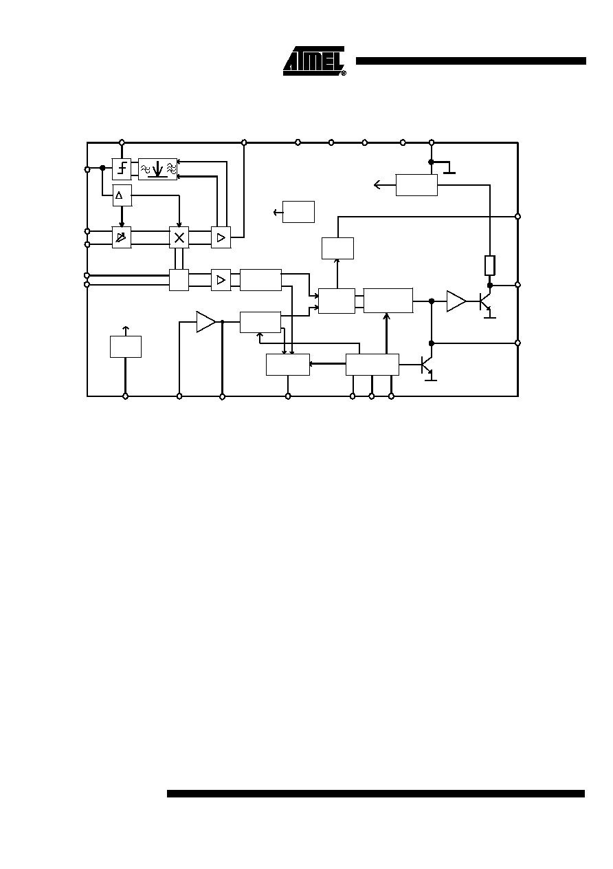
Figure 1. Block Diagram
Power
down
Power save
RF counter
: 2464
Reference
counter
: Nref
Tristate
phase
detector
Control
interface
20k
Test
interface
Lock
detector
Voltage
stabilizer
VCO
U
for frequency synthesizer
Band-
gap
Analog
part
PSM
TI
CI SI1
SI2
PD
CD
GND
PLCK
OSCB
NRF
RF
AGC
18
26
25
TH
17
IF
19
9
VCC2
20
VCC3
3
VCC1
28
VCC4
6, 7, 8, 21,
22, 23, 24
14
12
13
2
27
10
11
OSCE
16
15
1
TANK
VREF
5
4
Internal 5 V supply voltage
(analog part)
Charge
pump
200
m
/300
m
3
U2730B-N
4719A≠DAB≠05/03
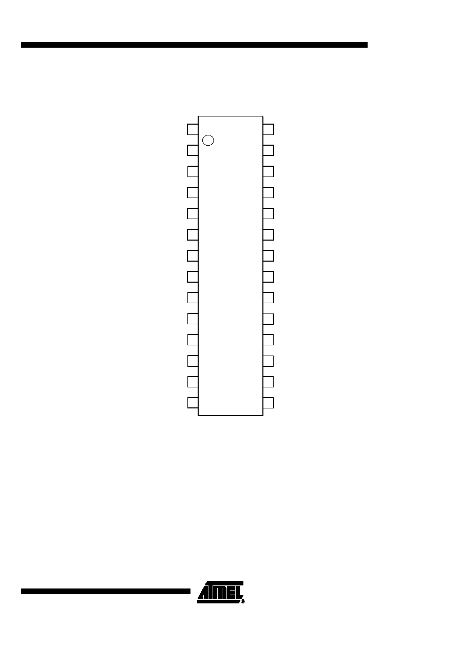
Pin Configuration
Figure 2. Pinning SSO28
GND
GND
VCC2
CI
TI
CD
PD
PLCK
1
2
3
4
5
6
7
8
10
9
27
22
21
20
18
19
17
12
11
28
25
26
23
24
GND
GND
GND
VCC3
IF
AGC
NRF
GND
TH
RF
SI1
VCC4
16
15
14
13
OSCE
OSCB
PSM
SI2
VCC1
VREF
TANK
GND
4
U2730B-N
4719A≠DAB≠05/03
Pin Description
Pin
Symbol
Function
1
PSM
Power save mode
2
SI2
Control input
3
VCC1
Supply voltage VCO
4
VREF
Reference pin of VCO
5
TANK
Tank pin of VCO
6, 7, 8, 21,
22, 23, 24
GND
Ground
9
VCC2
Supply voltage PLL
10
CI
Control input
11
TI
Test interface
12
CD
Active filter output
13
PD
Tristate charge pump output
14
PLCK
Lock-indication output (open collector)
15
OSCB
Input of internal oscillator/buffer
16
OSCE
Output of internal oscillator/buffer
17
TH
Threshold voltage of comparator
18
AGC
Charge-pump output of comparator, AGC input for amplifier and mixer
19
IF
Intermediate frequency output
20
VCC3
Supply voltage
25
NRF
RF input (inverted)
26
RF
RF input
27
SI1
Control input
28
VCC4
Supply voltage

5
U2730B-N
4719A≠DAB≠05/03
Functional Description
The U2730B-N is an L-band down-converter circuit covering a gain-controlled amplifier,
a gain-controlled mixer, an output buffer, a gain control circuitry, an L-band oscillator
and a frequency synthesizer block. Designed for applications in a DAB receiver, the cir-
cuit down-converts incoming L-band signals in the frequency range of 1452 MHz to
1492 MHz to an IF frequency in a range of 190 MHz to 230 MHz which can be handled
by a subsequent DAB tuner. A block diagram of this circuit is shown in Figure 1.
Gain-controlled Amplifier
RF signals applied to the 'RF' input pin are amplified by a gain-controlled amplifier. The
complementary pin NRF is not internally blocked, it is recommended to block this pin
carefully by an external capacitor. The gain-control voltage is generated by an internal
gain-control circuitry. The output signal of this amplifier is fed to a gain-controlled mixer.
Gain-controlled Mixer
and Output Buffer
The purpose of this mixer is to down-convert the L-band signal in the frequency range of
1452 MHz to 1492 MHz to an IF frequency in the range of about 190 MHz to 230 MHz.
Like the amplifier, the gain of the mixer is controlled by the gain-control circuitry. The IF
signal is buffered and filtered by a one-pole low-pass filter at a 3 dB frequency of about
500 MHz, and then it is fed to the single-ended output pin IF.
Gain-control Circuitry
The gain-control circuitry measures the signal power, compares it with a certain power
level and generates control voltages for the gain-controlled amplifier and mixer. An
equivalent circuit of this functional block is shown in Figure 6.
In order to meet this functionality, the output signal of the buffer amplifier is weakly
band-pass filtered (transition range of about 60 MHz to 550 MHz), rectified, low-pass fil-
tered and fed to a comparator whose threshold can be defined by an external resistor,
RTH, at pin TH. By varying the value of this resistor, a power threshold of about -33 dBm
to -20 dBm can be selected. In order to achieve a good intermodulation ratio, it is recom-
mended to keep the power threshold below -25 dBm. An appropriate application is
shown in Figure 3. Depending on the selection made by the comparator, a charge pump
charges or discharges a capacitor which is applied to the AGC pin. By varying this
capacitor, different time constants of the AGC loop can be realized. The voltage arising
at the AGC pin is used to control the gain setting of the gain-controlled amplifier and
mixer. The voltage at pin AGC is in the range of 5.75 V for maximum gain and 0.3 V for
minimum gain. This voltage can be use to control a dual-gate GaAs-FET in front of the
U2730B-N to achieve an extended AGC range. By applying an external voltage to the
AGC pin, the internal AGC loop can be overdriven.
Voltage-controlled
Oscillator
A voltage-controlled oscillator supplies a LO signal to the mixer. An equivalent circuit of
this oscillator is shown in Figure 7. In the application circuits Figure 8 and Figure 9, a
ceramic coaxial resonator is applied to the oscillator's TANK and VREF pins. It should
be noted that V
ref
has to be blocked carefully. Figure 9 shows a different application
where the oscillator is overdriven by an external oscillator. In any case, a DC path at a
low impedance must be established between the TANK and VREF pins. The output sig-
nal of the oscillator is fed to the LO divider block of the frequency synthesizer unit which
locks the VCO's frequency on the frequency of a reference oscillator. Figure 5 shows
the typical phase-noise performance of the oscillator in locked state.