U2741B
Rev. A2, 22-Dec-00
1 (7)
UHF ASK/FSK Transmitter
Description
The U2741B is a PLL transmitter IC which has been
specially developed for the demands of RF low-cost data
transmission systems at data rates up to 20 kBaud.
The transmitting frequency range is 300 MHz to
450 MHz. It can be used in both FSK and ASK systems.
Electrostatic sensitive device.
Observe precautions for handling.
Features
D One-chip solution with minimum external circuitry
D Lower cost than the usual discrete solutions using
SAW and transistors
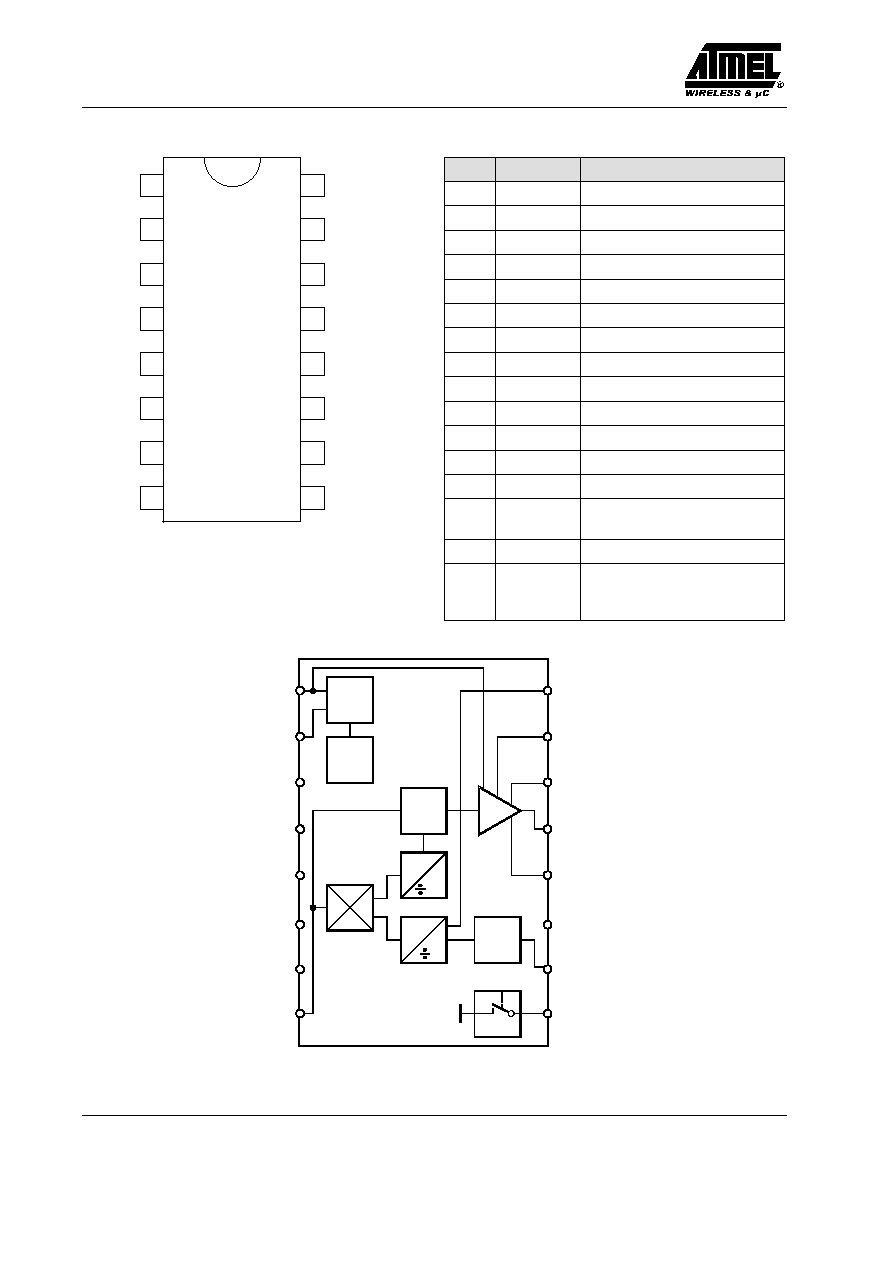
D Very small SSO16 package, pitch 0.635, 150 mil
D Supply voltage 2.0 V to 5.5 V
in the temperature range ≠20
∞
C to 70
∞
C
Supply voltage 2.2 V to 5.5 V
in the temperature range ≠40
∞
C to 85
∞
C
D "Single-Ended Open-Collector" output (same anten-
nas can be used as in discrete solutions, simpler
adaptation of magnetic loop antennas)
D XTO output for clocking the mC, thereby together
with M44C090 or M44C890 the optimum system
cost-effectiveness
D Very large FSK frequency deviation achievable by
±
100 ppm pulling of the reference crystal
D Very high transmitting frequency accuracy compared
to SAW solutions. This enables receivers at lower
bandwidth than is possible with SAW resonators.
D ESD protection according to MIL-STD.883
(4KV HBM) except Pins XTO1/ 2, ANT and LF
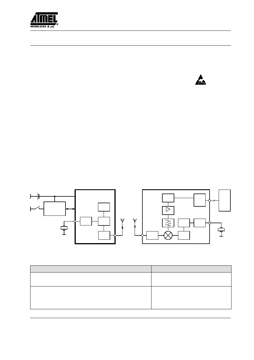
System Block Diagram
Demod.
IF Amp
LNA
VCO
PLL
XTO
Control
U3741BM
1...3
mC
Power
amp.
XTO
VCO
PLL
U2741B
Antenna Antenna
UHF ASK/FSK
Remote control transmitter
UHF ASK/FSK
Remote control receiver
Encoder
M44Cx9x
1 Li cell
Keys
Figure 1. System block diagram
Order Information
Extended Type Number
Package
Remarks
U2741B-MFB
SSO16
Tube
U2741B-MFBG3
SSO16
Taped and reeled
U2741B-NFB
SSO16
Tube, optimized power-supply rejection,
value of C
4
differs from M-version, en-
hanced XTO stability
U2741B-NFBG3
SSO16
Taped and reeled, see above
U2741B
Rev. A2, 22-Dec-00
3 (7)
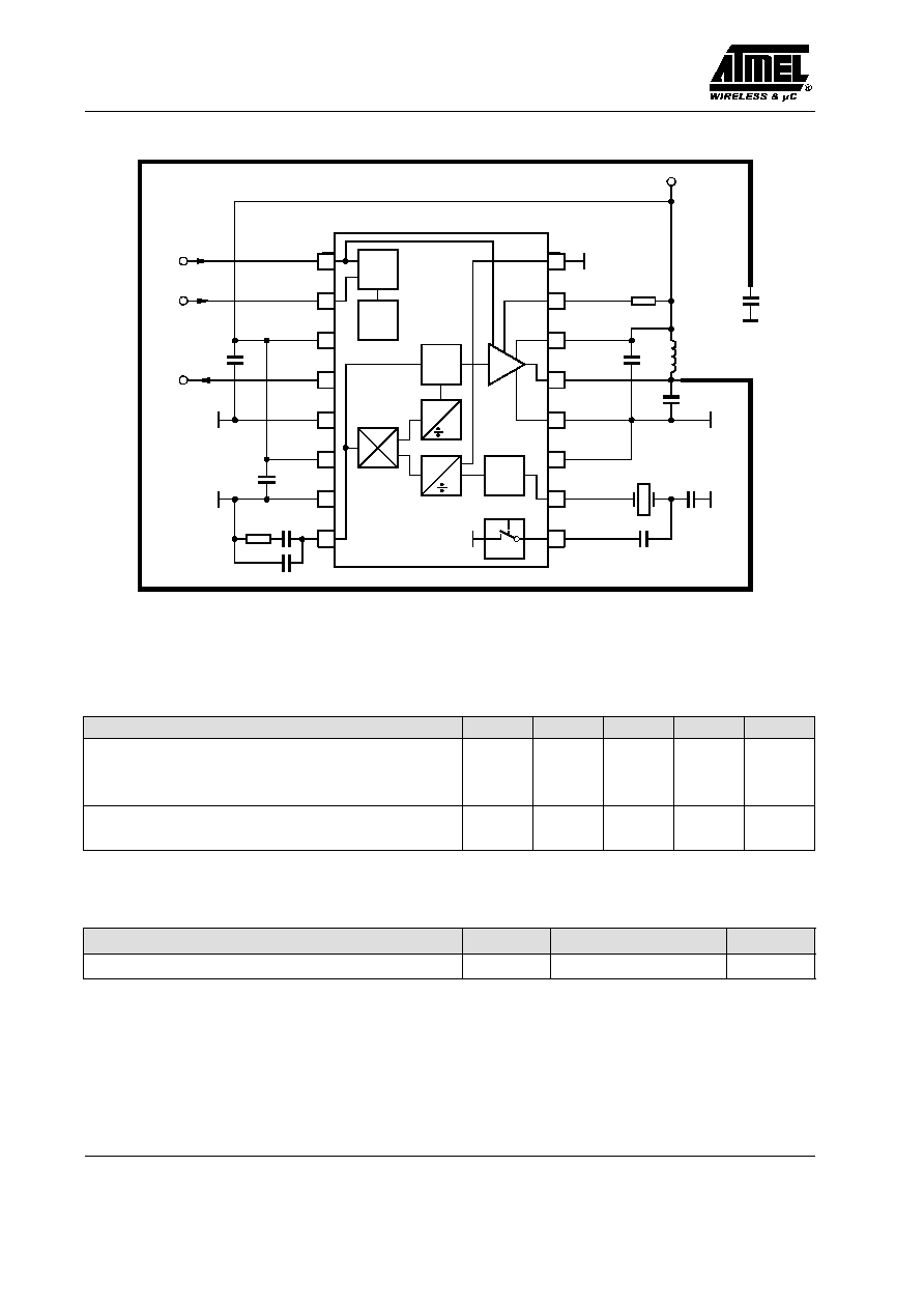
General Description
The fully integrated VCO and the "single-ended open-
collector" output allow particularly simple, low-cost RF
miniature transmitters to be assembled. The single-ended
output enables a considerably simplified adaptation of
both a magnetic loop antenna of any form or a
l/4
antenna. This is because the load impedance must not be
balanced as would be the case with a differential output.
The XTO's frequency can be selected at either 13.56 MHz
(USA 9.844 MHz) or 6.78 MHz (USA 4.9219 MHz).
Thus, it is possible to use not only exceptionally small SMD
crystals at 13.56 MHz but also very low-cost 6.78-MHz
crystals in a wired metal package (e.g. in the HC49S
housing). The frequency is selected by connecting PIN16
(DIVC) to either GND or V
S
.
At high frequencies, crystals have a very fast start-up time
(< 1.5 ms at 13.56 MHz, < 3 ms at 6.78 MHz), whereby
a wait time of 5 to 10 ms is required until the transmitter
IC is locked. This means that the processor does not need
to poll a lock detect output.
Functional Description
The IC can be switched on at both the FSK and the ASK
input. The IC's ChipSelect is performed by the logical OR
operation of ASK and FSK input. In the case of
V
FSK
, V
ASK
0.3 V, the power-down supply current is
IS
off
< 0.35
µ
A. The ASK input activates the power
amplifier and the PLL. The FSK input only activates the
PLL and, if capacitor C3 is installed, pulls the crystal to the
lower frequency, whereby the transmitter is FSK
modulated. After switching on at FSK, the VCO locks onto
the 32 or 64 times higher frequency of the crystal oscillator.
FSK Transmission
The U2741B is switched on by V
FSK
= V
S
. 5 ms later, V
S
is applied to V
ASK
. The output can then be modulated by
means of Pin FSK. This is done by connecting capacitor
C3 in parallel to the load capacitor C4.
ASK Transmission
The U2741B is activated by V
FSK
= V
S
. V
ASK
remains
0 V for 5 ms, then the output power can be modulated by
means of Pin ASK. In this case, V
FSK
remains = V
S
during
the message, the capacitor C3 is not mounted.
Take-Over of the Clock Pulse in the
µ
C
The clock of the crystal oscillator can be used for clocking
the
µ
C. The M44C090 and M44C890 have the special
feature of starting with an integrated RC oscillator to
switch on the U2741B with V
FSK
= V
S
. 5 ms later, the
3.39-MHz clock frequency is present, so that the message
can be sent with crystal accuracy.
Application Circuit
The following component values are recommendations
for a typical application. C5, C6, C7 are block capacitors.
The values of these capacitors depend on the board
layout. C5 = 1 nF, C6 = 1 nF, C7 = 22 nF are typically used
here. For C5, the impedance between f = 100 MHz and
f = 1 GHz should be as low as possible.
C3 is not needed in ASK transmitter applications. In the
case of FSK, C3 is selected in such a way that the desired
transmission frequency deviation is achieved (typ.
±
30 kHz). The capacitance here depends upon the
crystal's load capacity (C4) recommended by the
manufacturer of the crystal. C2 = 3.9 nF, C1 = 15 nF,
R4 = 220
W.
CLoop1, CLoop2 are selected so that the antenna
oscillates in resonance and the adaptation to the
appropriate impedance transformation is possible.
LFeed is an inductor for the antenna's DC current supply.
A typical value is LFeed = 220 nH. LFeed can be either
printed on the PC_Board or be a discrete component.
Further information regarding the application is provided
in the description of the "RKE Design Kit (U2741B,
U3741B)" in chapter 2.2.2. This chapter labeled
"Application Hints U2741B" also describes the antenna
design in more detail.
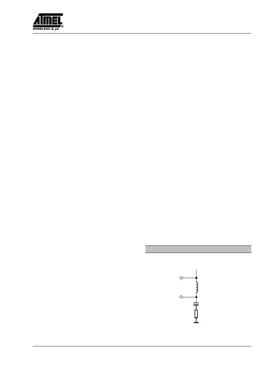
Output Power Measurement
The following output network (see figure 4) can be used
for output power evaluation, the exact values of L10, C10
are dependent on the layout.
L10, C10 is the transformation network to adopt the
output impedance of the IC to 50
W. The following table
shows the values for an output power of 2 mW and an
R
PWRSET
= 1.2 k
W.
f/ MHz
C10/ pF
L10/ nH
Z
Load_opt
/
W
315
2.7
56
260 + j330
433.92
1.8
33
185 + j268
15009
PWRVCC
ANT
V
S
L10
C10
50
W
Z
Load-opt
Figure 4. Measurement output network
U2741B
Rev. A2, 22-Dec-00
5 (7)
Electrical Characteristics
All parameters are refered to GND (Pin 5).
The possible operating ranges refer to different circuit conditions:
V
S
= 2.0 V to 5.5 V @ T
amb
= ≠20
∞
C to +70
∞
C, V
S
= 2.2 V to 5.5 V @ T
amb
= ≠40
∞
C to +85
∞
C (Typ. 25
∞
C, 3 V)
Parameters
Test Conditions / Pins
Symbol
Min.
Typ.
Max.
Unit
Supply current (power down) V
ASK
, V
FSK
v 0.3 V, V
S
< 3.6 V
IS
off
0.35
µ
A
Supply current
(power up, output OFF)
V
ASK
= GND, V
FSK
= V
S
, V
s
= 3 V
IS
on
4.7
6.2
mA
Supply current
(power up, output ON)
V
ASK
= V
S
, V
S
= 3 V
R
PWRSET
= 1.2 k
W
IS
transmit
10
12.5
mA
Output power
V
S
= 3 V, T
amb
= 25
∞
C,
f = 433.92 MHz
R
PWRSET
= 1.2 k
W
R
PWRSET
= 1.8 k
W
P
Ref
P
Ref
1.5
≠0.5
3
1
5
3
dBm
dBm
Output power variation for
the full temperature range
T
amb
= ≠40
∞
C to +85
∞
C,
f = 433.92 MHz, V
S
= 3.0 V
V
S
= 2.4 V
T
amb
= ≠20
∞
C to +85
∞
C,
f = 433.92 MHz, V
S
= 2.0 V
P
out
= P
Ref
+
DP
Ref
DP
Ref
DP
Ref
DP
Ref
≠1.5
≠4.0
≠5.5
dB
dB
dB
Output power variation for
f = 315 MHz compared to
f = 433.92 MHz
f = 315 MHz
P
out
= P
Ref
+
DP
Ref
DP
Ref
1.5
dB
Maximum peak output
antenna voltage
@
P
out
= 2.0 mW,
The load impedance must be selected
to meet the V
out
maximum requirement.
The supply current is not dependent on
the load impedance tolerance.
V
outmax
V
S
≠ 0.7 V
V
(peak)
Spurious emission
@ T
amb
= 25
∞
C
f
o
±
n
◊
f
PC
(f
PC
= 6.78 MHz)
Load capacitance at CLK
3 pF
f = 230 MHz to 470 MHz
f < 230 MHz, f > 470 MHz
Em
Em
≠40
≠58
dBC
dBC
Oscillator frequency XTO
M-version: @ T
amb
= 25
∞
C
N-version: full temperature range
(monitoring)
Crystal frequency = 13.56 MHz
6.78 MHz
load capacity of the crystal must be
selected accordingly
f
XTO
f
XTO
13.56
≠ 30 ppm
6.78
≠30 ppm
13.56
6.78
13.56
+30 ppm
6.78
+30 ppm
MHz
MHz
Loop bandwidth
For best LO noise
Loop filter components:
C2 = 3.9 nF, C1 = 15 nF, R4 = 220
W
B
Loop
100
kHz
Phase noise PLL
Referring to the phase comparator
f
PC
= 6.78 MHz
PN
PLL
≠111
≠105
dBC/Hz
Phase noise VCO
@ 1 MHz
@ 36 MHz
PN
VCO
PN
VCO
≠91
≠123
≠87
≠119
dBC/Hz
Frequency range of the VCO
f
VCO
300
450
MHz
Clock output
(CMOS
µ
C compatible)
Clk
out
f
out
/128
MHz