Rev. 4733A≠RKE≠11/03
Features
∑
Very High Transmitting Frequency Accuracy Compared to SAW Solutions
(Enables Receivers at Lower Bandwidth than with SAW Resonators)
∑
Lower Cost than the Usual Discrete Solutions Using SAW and Transistors
∑
Supply Voltage 2.0 V to 5.5 V in the Temperature Range -20
∞
C to 70
∞
C
Supply Voltage 2.2 V to 5.5 V in the Temperature Range -40
∞
C to 85
∞
C
∑
XTO Output for Clocking the Microcontroller, Thereby Together with the ATAR090 or
ATAR890 Results in the Optimum System Cost-effectiveness
∑
One-chip Solution with Minimum External Circuitry
∑
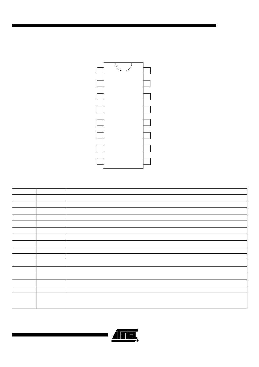
Very Small SSO16 Package, Pitch 0.635, 150 mil
∑
"Single-ended Open-collector" Output (Same Antennas as in Discrete Solutions Can
Be Used, Simpler Adaptation of Magnetic Loop Antennas)
∑
Very Large FSK Frequency Deviation Achievable by ±100 ppm Pulling of the Reference
Crystal
∑
Enables Receivers at Lower Bandwidth than with SAW Resonators
∑
ESD Protection According to MIL-STD.883 (4 KV HBM) Except Pins XTO1/ 2,
ANT and LF
Electrostatic sensitive device.
Observe precautions for handling.
Description
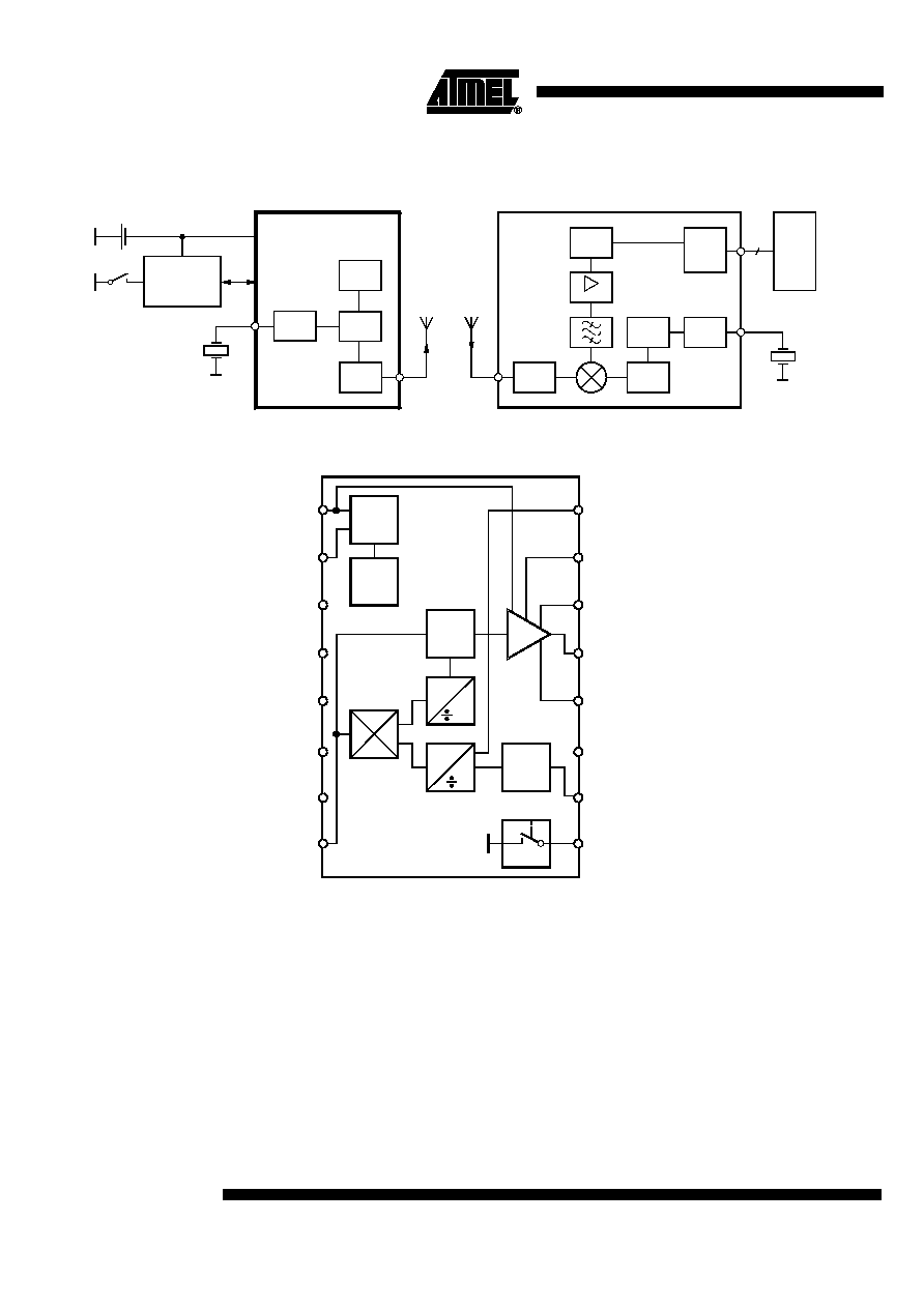
The U2741B is a PLL transmitter IC which has been especially developed for the
demands of RF low-cost data transmission systems at data rates up to 20 kBaud.
The transmitting frequency range is 300 MHz to 450 MHz. The device can be used in
both FSK and ASK systems.
UHF ASK/FSK
Transmitter
U2741B

4
U2741B
4733A≠RKE≠11/03
General Description
The fully integrated VCO and the "single-ended open-collector" output allow particularly
simple, low-cost RF miniature transmitters to be assembled. The single-ended output
enables a considerably simplified adaptation of both a magnetic loop antenna of any
form or a
l
/4 antenna. This is because the load impedance must not be balanced as
would be the case with a differential output.
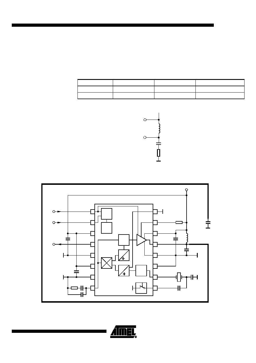
The XTO's frequency can be selected at either 13.56 MHz (USA 9.844 MHz) or
6.78 MHz (USA 4.9219 MHz). Thus, it is possible to use not only exceptionally small
SMD crystals at 13.56 MHz but also very low-cost 6.78 MHz crystals in a wired metal
package (e.g., in the HC49S housing). The frequency is selected by connecting pin 16
(DIVC) to either GND or V
S
.
At high frequencies, crystals have a very fast start-up time (< 1.5 ms at 13.56 MHz,
< 3 ms at 6.78 MHz), whereby a wait time of 5 to 10 ms is required until the transmitter
IC is locked. This means that the processor does not need to poll a lock detect output.
Functional
Description
The IC can be switched on at both the FSK and the ASK input. The IC's ChipSelect is
performed by the logical OR operation of ASK and FSK input. In the case of V
FSK
,
V
ASK
£
0.3 V, the power-down supply current is IS
off
< 0.35 µA. The ASK input activates
the power amplifier and the PLL. The FSK input only activates the PLL and, if capacitor
C
3
is installed, pulls the crystal to the lower frequency, whereby the transmitter is FSK
modulated. After switching on at FSK, the VCO locks onto the 32 or 64 times higher fre-
quency of the crystal oscillator.
FSK Transmission
The U2741B is switched on by V
FSK
= V
S
. 5 ms later, V
S
is applied to V
ASK
. The output
can then be modulated by means of pin FSK. This is done by connecting capacitor C
3
in
parallel to the load capacitor C
4
.
ASK Transmission
The U2741B is activated by V
FSK
= V
S
. V
ASK
remains 0 V for 5 ms, then the output power
can be modulated by means of pin ASK. In this case, V
FSK
remains = V
S
during the mes-
sage, the capacitor C
3
is not mounted.
Take-over of the Clock
Pulse in the
Microcontroller
The clock of the crystal oscillator can be used for clocking the microcontroller. The
ATAR090 and ATAR890 have the special feature of starting with an integrated RC oscil-
lator to switch on the U2741B with V
FSK
= V
S
. 5 ms later, the 3.39-MHz clock frequency
is present, so that the message can be sent with crystal accuracy.
Application Circuit
The following component values are recommendations for a typical application. C
5
, C
6
,
and C
7
are block capacitors. The values of these capacitors depend on the board layout.
C
5
= 1 nF, C
6
= 1 nF, and C
7
= 22 nF are typically used here. For C
5
, the impedance
between f = 100 MHz and f = 1 GHz should be as low as possible.
C
3
is not needed in ASK transmitter applications. In the case of FSK, C
3
is selected in
such a way that the desired transmission frequency deviation is achieved (typical
±30 kHz). The capacitance here depends upon the crystal's load capacity (C
4
) recom-
mended by the manufacturer of the crystal. C
2
= 3.9 nF, C
1
= 15 nF, and R
4
= 220
W
.
C
Loop1
and C
Loop2
are selected so that the antenna oscillates in resonance and the adap-
tation to the appropriate impedance transformation is possible.
L
F e e d
is an inductor for the antenna's DC current supply. A typical value is
L
Feed
= 220 nH. L
Feed
can be either printed on the PC board or be a discrete component.