U2786B
Preliminary Information
Rev. A2, 18≠Aug≠00
1 (17)
DECT PLL / TX IC
Description
The U2786B is an RF IC for low-power DECT transmit
applications. The IC includes a complete PLL with
1-GHz prescaler, on-chip frequency doubler, biasing for
off-chip VCO, an integrated TX filter and a modulation-
compensation circuit for advanced closed-loop
modulation concept.
Electrostatic sensitive device.
Observe precautions for handling.
Features
D 1-GHz PLL, frequency doubler, TX data filter
(13.824-MHz/ 27.648-MHz reference clock)
D Supply-voltage range: 2.7 V to 4.7 V
D Low current consumption
D Few external components
D No mechanical tuning necessary
D Switchable charge-pump current for enhanced
switching time
D 1 operational amplifier for active loop filter
D Advanced closed-loop modulation (with
13.824-MHz/ 27.648-MHz reference clock) and open
loop modulation supported
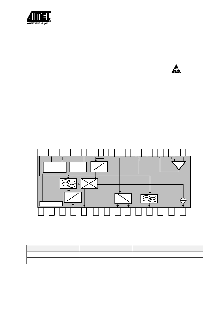
Block Diagram
DAC
VS
FD_OUT1
I_CP_SW
DATA
OLE
LD
OP_OUT
n.c.
PU_MIN
OP_N
OP_P
GND_D
ENABLE
CLOCK
REF_CLK
GND_RF_IN
PU
TX_DATA
GND_FD_OUT
RF_IN
FD_OUT2
GF_DATA
CP
VS_CP
GND_CP
VCO_BIAS
GND_OP
FD
f
PD
f
: n
OP
MCC
GF
Control logic
RC
PC
CP
2f
f
3-wire bus
: n
DAC
3
4
5
6
7
8
9
10
11
12
13
14
15
16
17
18
19
20
21
22
23
24
25
26
27
28
+
≠
1
2
14224
Figure 1. Block diagram
Ordering Information
Extended Type Number
Package
Remarks
U2786B-MFS
SSO28
Tube
U2786B-MFSG3
SSO28
Taped and reeled
U2786B
Preliminary Information
Rev. A2, 18≠Aug≠00
3 (17)
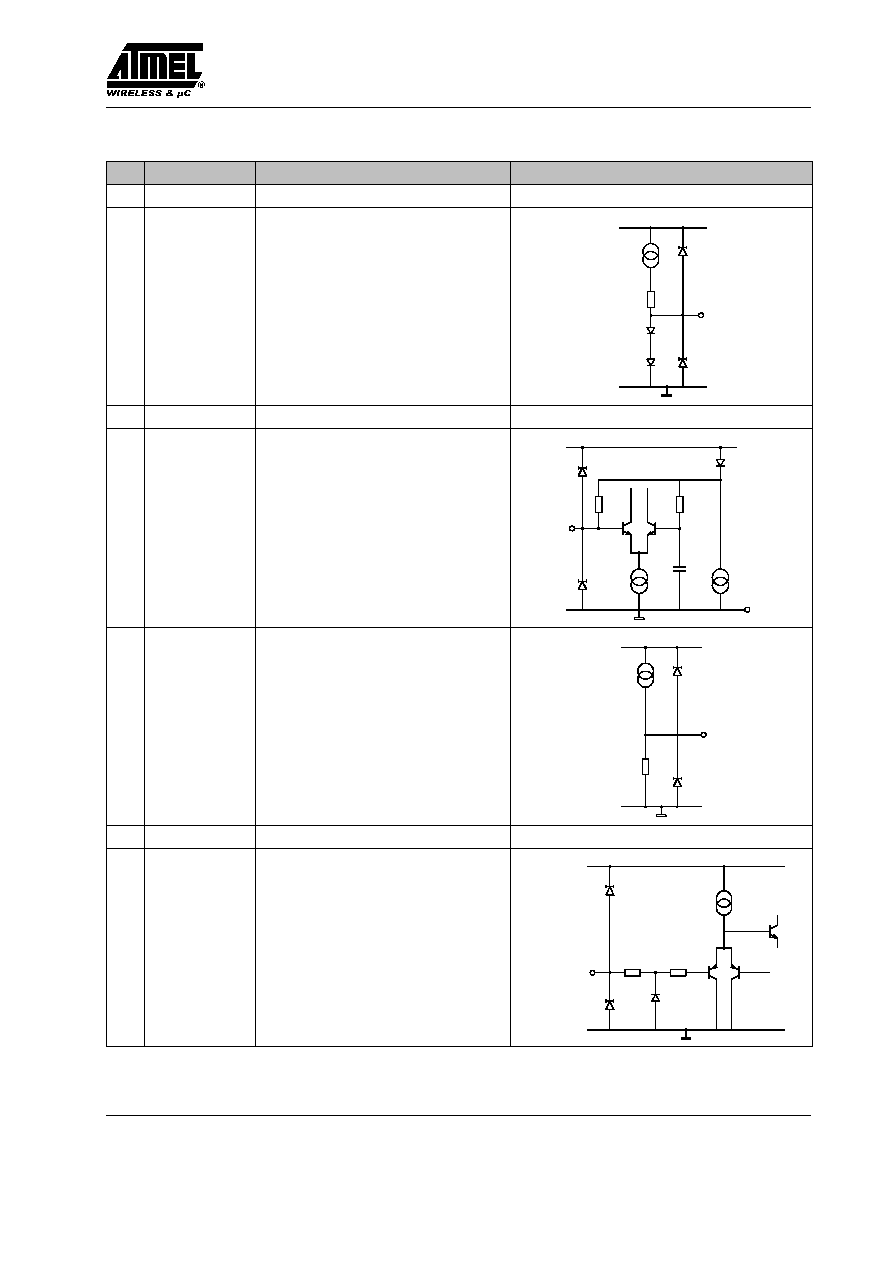
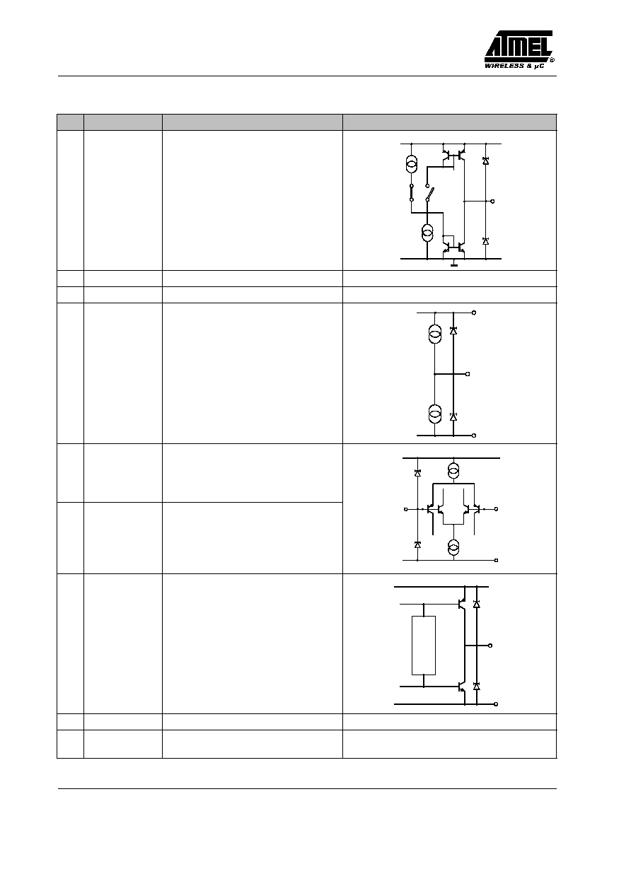
Pin Description (continued)
Pin
Symbol
Function
Configuration
¡¡¡
¡¡¡
¡¡¡
¡¡¡
¡¡¡
¡¡¡
¡¡¡
¡¡¡
¡¡¡
4
¡¡¡¡¡
¡¡¡¡¡
¡¡¡¡¡
¡¡¡¡¡
¡¡¡¡¡
¡¡¡¡¡
¡¡¡¡¡
¡¡¡¡¡
¡¡¡¡¡
REF_CLK
¡¡¡¡¡¡¡¡¡¡¡¡
¡¡¡¡¡¡¡¡¡¡¡¡
¡¡¡¡¡¡¡¡¡¡¡¡
¡¡¡¡¡¡¡¡¡¡¡¡
¡¡¡¡¡¡¡¡¡¡¡¡
¡¡¡¡¡¡¡¡¡¡¡¡
¡¡¡¡¡¡¡¡¡¡¡¡
¡¡¡¡¡¡¡¡¡¡¡¡
¡¡¡¡¡¡¡¡¡¡¡¡
Reference frequency input
¡¡¡¡¡¡¡¡¡¡¡¡¡¡
¡¡¡¡¡¡¡¡¡¡¡¡¡¡
¡¡¡¡¡¡¡¡¡¡¡¡¡¡
¡¡¡¡¡¡¡¡¡¡¡¡¡¡
¡¡¡¡¡¡¡¡¡¡¡¡¡¡
¡¡¡¡¡¡¡¡¡¡¡¡¡¡
¡¡¡¡¡¡¡¡¡¡¡¡¡¡
¡¡¡¡¡¡¡¡¡¡¡¡¡¡
¡¡¡¡¡¡¡¡¡¡¡¡¡¡
VS
10k
10k
4
¡¡¡
¡¡¡
¡¡¡
¡¡¡
¡¡¡
¡¡¡
¡¡¡
¡¡¡
¡¡¡
¡¡¡
5
¡¡¡¡¡
¡¡¡¡¡
¡¡¡¡¡
¡¡¡¡¡
¡¡¡¡¡
¡¡¡¡¡
¡¡¡¡¡
¡¡¡¡¡
¡¡¡¡¡
¡¡¡¡¡
LD
¡¡¡¡¡¡¡¡¡¡¡¡
¡¡¡¡¡¡¡¡¡¡¡¡
¡¡¡¡¡¡¡¡¡¡¡¡
¡¡¡¡¡¡¡¡¡¡¡¡
¡¡¡¡¡¡¡¡¡¡¡¡
¡¡¡¡¡¡¡¡¡¡¡¡
¡¡¡¡¡¡¡¡¡¡¡¡
¡¡¡¡¡¡¡¡¡¡¡¡
¡¡¡¡¡¡¡¡¡¡¡¡
¡¡¡¡¡¡¡¡¡¡¡¡
Lock detect output
¡¡¡¡¡¡¡¡¡¡¡¡¡¡
¡¡¡¡¡¡¡¡¡¡¡¡¡¡
¡¡¡¡¡¡¡¡¡¡¡¡¡¡
¡¡¡¡¡¡¡¡¡¡¡¡¡¡
¡¡¡¡¡¡¡¡¡¡¡¡¡¡
¡¡¡¡¡¡¡¡¡¡¡¡¡¡
¡¡¡¡¡¡¡¡¡¡¡¡¡¡
¡¡¡¡¡¡¡¡¡¡¡¡¡¡
¡¡¡¡¡¡¡¡¡¡¡¡¡¡
¡¡¡¡¡¡¡¡¡¡¡¡¡¡
VS
100
5
¡¡¡
¡¡¡
¡¡¡
¡¡¡
¡¡¡
¡¡¡
¡¡¡
¡¡¡
¡¡¡
¡¡¡
6
¡¡¡¡¡
¡¡¡¡¡
¡¡¡¡¡
¡¡¡¡¡
¡¡¡¡¡
¡¡¡¡¡
¡¡¡¡¡
¡¡¡¡¡
¡¡¡¡¡
¡¡¡¡¡
I_CP_SW
¡¡¡¡¡¡¡¡¡¡¡¡
¡¡¡¡¡¡¡¡¡¡¡¡
¡¡¡¡¡¡¡¡¡¡¡¡
¡¡¡¡¡¡¡¡¡¡¡¡
¡¡¡¡¡¡¡¡¡¡¡¡
¡¡¡¡¡¡¡¡¡¡¡¡
¡¡¡¡¡¡¡¡¡¡¡¡
¡¡¡¡¡¡¡¡¡¡¡¡
¡¡¡¡¡¡¡¡¡¡¡¡
¡¡¡¡¡¡¡¡¡¡¡¡
Charge-pump current switch
¡¡¡¡¡¡¡¡¡¡¡¡¡¡
¡¡¡¡¡¡¡¡¡¡¡¡¡¡
¡¡¡¡¡¡¡¡¡¡¡¡¡¡
¡¡¡¡¡¡¡¡¡¡¡¡¡¡
¡¡¡¡¡¡¡¡¡¡¡¡¡¡
¡¡¡¡¡¡¡¡¡¡¡¡¡¡
¡¡¡¡¡¡¡¡¡¡¡¡¡¡
¡¡¡¡¡¡¡¡¡¡¡¡¡¡
¡¡¡¡¡¡¡¡¡¡¡¡¡¡
¡¡¡¡¡¡¡¡¡¡¡¡¡¡
VS
Ref
(10k)
6
5k
(10k)
5k
¡¡¡
¡¡¡
7
¡¡¡¡¡
¡¡¡¡¡
GND_FD_OUT
¡¡¡¡¡¡¡¡¡¡¡¡
¡¡¡¡¡¡¡¡¡¡¡¡
Frequency-doubler buffer ground
¡¡¡¡¡¡¡¡¡¡¡¡¡¡
¡¡¡¡¡¡¡¡¡¡¡¡¡¡
¡¡¡
¡¡¡
¡¡¡
¡¡¡
¡¡¡
8
¡¡¡¡¡
¡¡¡¡¡
¡¡¡¡¡
¡¡¡¡¡
¡¡¡¡¡
FD_OUT1
¡¡¡¡¡¡¡¡¡¡¡¡
¡¡¡¡¡¡¡¡¡¡¡¡
¡¡¡¡¡¡¡¡¡¡¡¡
¡¡¡¡¡¡¡¡¡¡¡¡
¡¡¡¡¡¡¡¡¡¡¡¡
Frequency-doubler buffer output 1
¡¡¡¡¡¡¡¡¡¡¡¡¡¡
¡¡¡¡¡¡¡¡¡¡¡¡¡¡
¡¡¡¡¡¡¡¡¡¡¡¡¡¡
¡¡¡¡¡¡¡¡¡¡¡¡¡¡
¡¡¡¡¡¡¡¡¡¡¡¡¡¡
VS
¡¡¡
¡¡¡
¡¡¡
¡¡¡
¡¡¡
9
¡¡¡¡¡
¡¡¡¡¡
¡¡¡¡¡
¡¡¡¡¡
¡¡¡¡¡
FD_OUT2
¡¡¡¡¡¡¡¡¡¡¡¡
¡¡¡¡¡¡¡¡¡¡¡¡
¡¡¡¡¡¡¡¡¡¡¡¡
¡¡¡¡¡¡¡¡¡¡¡¡
¡¡¡¡¡¡¡¡¡¡¡¡
Frequency-doubler buffer output 2
¡¡¡¡¡¡¡¡¡¡¡¡¡¡
¡¡¡¡¡¡¡¡¡¡¡¡¡¡
¡¡¡¡¡¡¡¡¡¡¡¡¡¡
¡¡¡¡¡¡¡¡¡¡¡¡¡¡
¡¡¡¡¡¡¡¡¡¡¡¡¡¡
8,9
7
¡¡¡
¡¡¡
10
¡¡¡¡¡
¡¡¡¡¡
VS
¡¡¡¡¡¡¡¡¡¡¡¡
¡¡¡¡¡¡¡¡¡¡¡¡
Supply voltage
¡¡¡¡¡¡¡¡¡¡¡¡¡¡
¡¡¡¡¡¡¡¡¡¡¡¡¡¡
U2786B
Rev. A2, 18≠Aug≠00
Preliminary Information
4 (17)
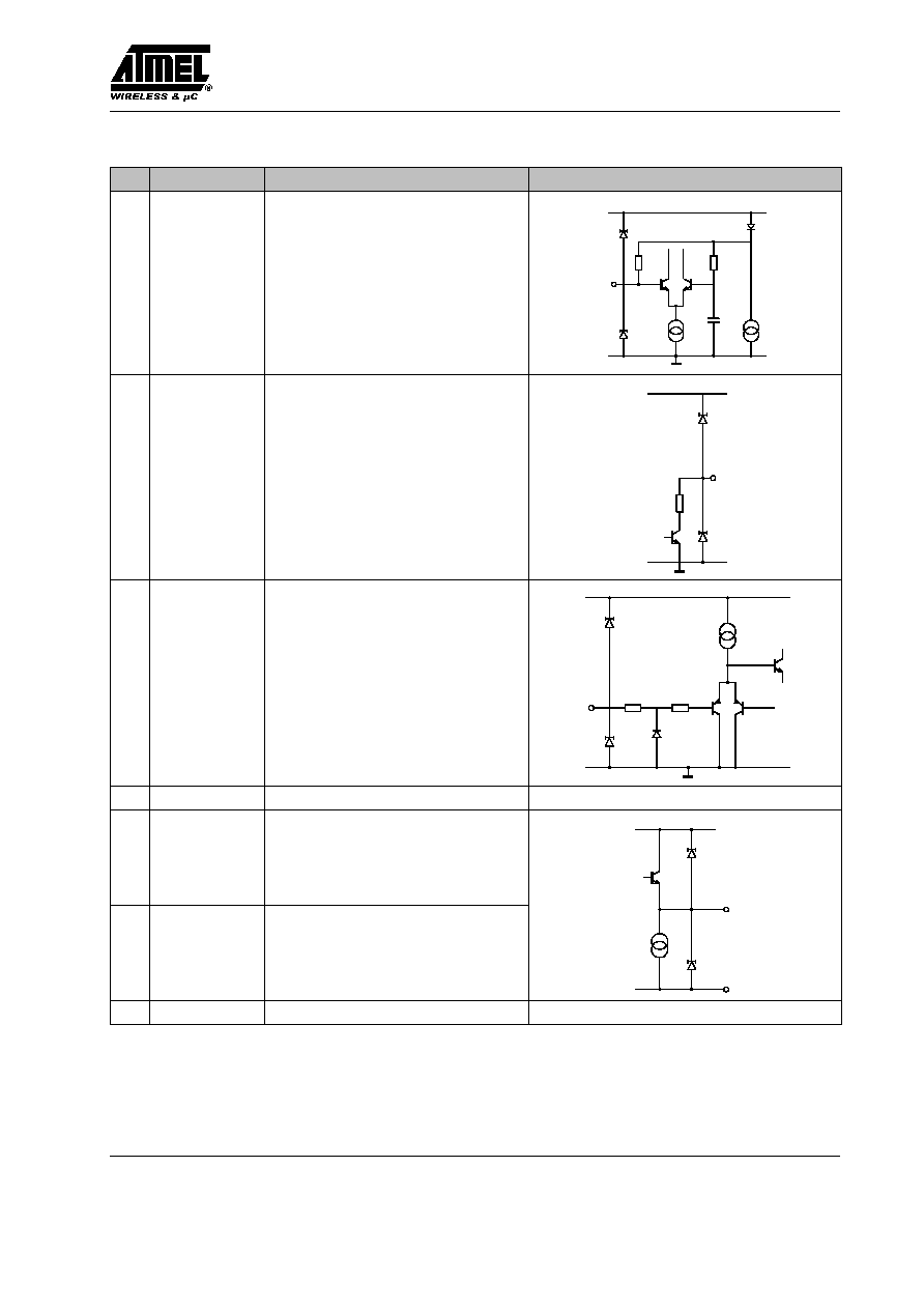
Pin Description (continued)
Pin
Symbol
Function
Configuration
¡¡¡
¡¡¡
¡¡¡
¡¡¡
¡¡¡
¡¡¡
¡¡¡
¡¡¡
¡¡¡
¡¡¡
11
¡¡¡¡¡
¡¡¡¡¡
¡¡¡¡¡
¡¡¡¡¡
¡¡¡¡¡
¡¡¡¡¡
¡¡¡¡¡
¡¡¡¡¡
¡¡¡¡¡
¡¡¡¡¡
GF_DATA
¡¡¡¡¡¡¡¡¡¡¡¡
¡¡¡¡¡¡¡¡¡¡¡¡
¡¡¡¡¡¡¡¡¡¡¡¡
¡¡¡¡¡¡¡¡¡¡¡¡
¡¡¡¡¡¡¡¡¡¡¡¡
¡¡¡¡¡¡¡¡¡¡¡¡
¡¡¡¡¡¡¡¡¡¡¡¡
¡¡¡¡¡¡¡¡¡¡¡¡
¡¡¡¡¡¡¡¡¡¡¡¡
¡¡¡¡¡¡¡¡¡¡¡¡
Modulation output
(Gaussian filtered data signal)
¡¡¡¡¡¡¡¡¡¡¡¡¡¡
¡¡¡¡¡¡¡¡¡¡¡¡¡¡
¡¡¡¡¡¡¡¡¡¡¡¡¡¡
¡¡¡¡¡¡¡¡¡¡¡¡¡¡
¡¡¡¡¡¡¡¡¡¡¡¡¡¡
¡¡¡¡¡¡¡¡¡¡¡¡¡¡
¡¡¡¡¡¡¡¡¡¡¡¡¡¡
¡¡¡¡¡¡¡¡¡¡¡¡¡¡
¡¡¡¡¡¡¡¡¡¡¡¡¡¡
¡¡¡¡¡¡¡¡¡¡¡¡¡¡
VS
11
¡¡¡
¡¡¡
12
¡¡¡¡¡
¡¡¡¡¡
GND_CP
¡¡¡¡¡¡¡¡¡¡¡¡
¡¡¡¡¡¡¡¡¡¡¡¡
Charge-pump ground
¡¡¡¡¡¡¡¡¡¡¡¡¡¡
¡¡¡¡¡¡¡¡¡¡¡¡¡¡
¡¡¡
¡¡¡
13
¡¡¡¡¡
¡¡¡¡¡
VS_CP
¡¡¡¡¡¡¡¡¡¡¡¡
¡¡¡¡¡¡¡¡¡¡¡¡
Charge-pump supply voltage
¡¡¡¡¡¡¡¡¡¡¡¡¡¡
¡¡¡¡¡¡¡¡¡¡¡¡¡¡
¡¡¡
¡¡¡
¡¡¡
¡¡¡
¡¡¡
¡¡¡
¡¡¡
¡¡¡
¡¡¡
14
¡¡¡¡¡
¡¡¡¡¡
¡¡¡¡¡
¡¡¡¡¡
¡¡¡¡¡
¡¡¡¡¡
¡¡¡¡¡
¡¡¡¡¡
¡¡¡¡¡
CP
¡¡¡¡¡¡¡¡¡¡¡¡
¡¡¡¡¡¡¡¡¡¡¡¡
¡¡¡¡¡¡¡¡¡¡¡¡
¡¡¡¡¡¡¡¡¡¡¡¡
¡¡¡¡¡¡¡¡¡¡¡¡
¡¡¡¡¡¡¡¡¡¡¡¡
¡¡¡¡¡¡¡¡¡¡¡¡
¡¡¡¡¡¡¡¡¡¡¡¡
¡¡¡¡¡¡¡¡¡¡¡¡
Charge-pump output
¡¡¡¡¡¡¡¡¡¡¡¡¡¡
¡¡¡¡¡¡¡¡¡¡¡¡¡¡
¡¡¡¡¡¡¡¡¡¡¡¡¡¡
¡¡¡¡¡¡¡¡¡¡¡¡¡¡
¡¡¡¡¡¡¡¡¡¡¡¡¡¡
¡¡¡¡¡¡¡¡¡¡¡¡¡¡
¡¡¡¡¡¡¡¡¡¡¡¡¡¡
¡¡¡¡¡¡¡¡¡¡¡¡¡¡
¡¡¡¡¡¡¡¡¡¡¡¡¡¡
13
14
12
¡¡¡
¡¡¡
¡¡¡
¡¡¡
¡¡¡
15
¡¡¡¡¡
¡¡¡¡¡
¡¡¡¡¡
¡¡¡¡¡
¡¡¡¡¡
OP_N
¡¡¡¡¡¡¡¡¡¡¡¡
¡¡¡¡¡¡¡¡¡¡¡¡
¡¡¡¡¡¡¡¡¡¡¡¡
¡¡¡¡¡¡¡¡¡¡¡¡
¡¡¡¡¡¡¡¡¡¡¡¡
Operational-amplifier inverting input
¡¡¡¡¡¡¡¡¡¡¡¡¡¡
¡¡¡¡¡¡¡¡¡¡¡¡¡¡
¡¡¡¡¡¡¡¡¡¡¡¡¡¡
¡¡¡¡¡¡¡¡¡¡¡¡¡¡
¡¡¡¡¡¡¡¡¡¡¡¡¡¡
VS
¡¡¡
¡¡¡
¡¡¡
¡¡¡
¡¡¡
16
¡¡¡¡¡
¡¡¡¡¡
¡¡¡¡¡
¡¡¡¡¡
¡¡¡¡¡
OP_P
¡¡¡¡¡¡¡¡¡¡¡¡
¡¡¡¡¡¡¡¡¡¡¡¡
¡¡¡¡¡¡¡¡¡¡¡¡
¡¡¡¡¡¡¡¡¡¡¡¡
¡¡¡¡¡¡¡¡¡¡¡¡
Operational-amplifier non-inverting
input
¡¡¡¡¡¡¡¡¡¡¡¡¡¡
¡¡¡¡¡¡¡¡¡¡¡¡¡¡
¡¡¡¡¡¡¡¡¡¡¡¡¡¡
¡¡¡¡¡¡¡¡¡¡¡¡¡¡
¡¡¡¡¡¡¡¡¡¡¡¡¡¡
18
16
15
¡¡¡
¡¡¡
¡¡¡
¡¡¡
¡¡¡
¡¡¡
¡¡¡
¡¡¡
¡¡¡
¡¡¡
17
¡¡¡¡¡
¡¡¡¡¡
¡¡¡¡¡
¡¡¡¡¡
¡¡¡¡¡
¡¡¡¡¡
¡¡¡¡¡
¡¡¡¡¡
¡¡¡¡¡
¡¡¡¡¡
OP_OUT
¡¡¡¡¡¡¡¡¡¡¡¡
¡¡¡¡¡¡¡¡¡¡¡¡
¡¡¡¡¡¡¡¡¡¡¡¡
¡¡¡¡¡¡¡¡¡¡¡¡
¡¡¡¡¡¡¡¡¡¡¡¡
¡¡¡¡¡¡¡¡¡¡¡¡
¡¡¡¡¡¡¡¡¡¡¡¡
¡¡¡¡¡¡¡¡¡¡¡¡
¡¡¡¡¡¡¡¡¡¡¡¡
¡¡¡¡¡¡¡¡¡¡¡¡
Operational-amplifier output
¡¡¡¡¡¡¡¡¡¡¡¡¡¡
¡¡¡¡¡¡¡¡¡¡¡¡¡¡
¡¡¡¡¡¡¡¡¡¡¡¡¡¡
¡¡¡¡¡¡¡¡¡¡¡¡¡¡
¡¡¡¡¡¡¡¡¡¡¡¡¡¡
¡¡¡¡¡¡¡¡¡¡¡¡¡¡
¡¡¡¡¡¡¡¡¡¡¡¡¡¡
¡¡¡¡¡¡¡¡¡¡¡¡¡¡
¡¡¡¡¡¡¡¡¡¡¡¡¡¡
¡¡¡¡¡¡¡¡¡¡¡¡¡¡
VS
17
18
AB-Control
¡¡¡
¡¡¡
18
¡¡¡¡¡
¡¡¡¡¡
GND_OP
¡¡¡¡¡¡¡¡¡¡¡¡
¡¡¡¡¡¡¡¡¡¡¡¡
Operational-amplifier ground
¡¡¡¡¡¡¡¡¡¡¡¡¡¡
¡¡¡¡¡¡¡¡¡¡¡¡¡¡
¡¡¡
¡¡¡
19
¡¡¡¡¡
¡¡¡¡¡
PU_MIN
¡¡¡¡¡¡¡¡¡¡¡¡
¡¡¡¡¡¡¡¡¡¡¡¡
3-wire bus: Data-hold enable in power-
down mode
¡¡¡¡¡¡¡¡¡¡¡¡¡¡
¡¡¡¡¡¡¡¡¡¡¡¡¡¡