
Rev. 4794A≠TVVCR≠02/04
Features
∑
Two Alignment-free PLL FM Demodulators, Automatic Lock-in on the Received Sound
Carrier Frequency
∑
Mono and Dual Channel Application
∑
Sound IF Inputs Provided for Ceramic Filters
∑
Automatic Mute for Second Sound Channel (Squelch)
∑
Mute Function for Both Sound Channels
∑
5-V Supply Voltage, Low-power Consumption
∑
Few External Components
Description
The U2860B-M is a dual-channel FM sound demodulator realized with Atmel 's
advanced bipolar process. All TV FM standards, from 4.5 MHz up to 6.5 MHz
(standard M, B/G, I, D/K) can be processed with high performance. The circuit is
alignment-free and has a minimum number of external components. With 5 V supply
voltage, the U2860B-M is suitable for TV, VCR and multimedia applications.
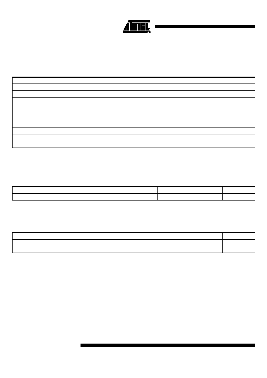
Figure 1. Block Diagram
Loop
filter 1
VCO 1
Mute
1
3
4
13
11
12
Supply
8
7
C
stab
VCO
offset
10
VCO offset
Loop
filter 2
VCO 1
V
S
Squelch
Squelch (second carrier)
14
Squelch
V
in1
Mute
V
AF1
V
AF2
6
9
R
ref
(optional)
V
in2
Dual-Channel
FM Sound
Demodulator for
TV Systems
U2860B-M

2
U2860B-M
4794A≠TVVCR≠02/04
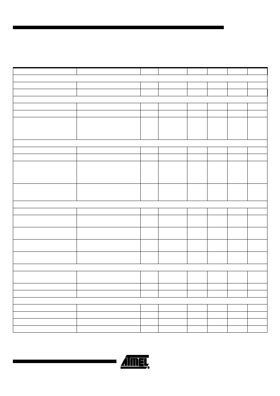
Pin Configuration
Figure 2. Pinning
V
in1
NC
V
mute
V
sque
NC
V
AF2
V
AF1
V
in2
V
S
GND
C
stab
R
ref
C
9
C
8
1
2
3
4
5
6
7
14
13
12
11
10
9
8
Pin Description
Pin
Symbol
Function
1
V
in1
Intercarrier input of sound channel 1 (5.5 MHz)
2
NC
Not connected
3
V
mute
Mute for sound channel 1+2 "on/off"
4
V
sque
Automatic mute for 2nd sound channel (squelch) "on/off"
5
NC
Not connected
6
V
AF2
Audio output AF2 of sound channel 2
7
V
AF1
Audio output AF1 of sound channel 1
8
C
8
Decoupling capacitor for sound channel 1
9
C
9
Decoupling capacitor for sound channel 2
10
R
ref
VCO offset of the free-running frequency
11
C
stab
Internal supply voltage stabilization
12
GND
Ground
13
V
S
Supply voltage
14
V
in2
Intercarrier input of sound channel 2 (5.74 MHz)

3
U2860B-M
4794A≠TVVCR≠02/04
Circuit Description
The U2860B-M includes two identical sound IF channels. Each consists of a limiter
amplifier, PLL FM demodulator and AF amplifier. Additionally, this circuit contains a
squelch function, mute switch and internal voltage regulation.
Limiter Amplifiers
The intercarrier signals are fed through external ceramic bandpass filters to a 7-stage
limiter amplifier. This guarantees high input sensitivity and excellent AM suppression.
PLL FM
Demodulators
The alignment-free Phase Locked Loop (PLL) demodulator covers a wide frequency
range of 4.5 MHz up to 6.5 MHz with low-noise performance. The linear voltage to
frequency characteristic results in low harmonic distortion. The free-running frequency
of the internal VCO circuit is about 5.5 MHz. For this frequency, the input sensitivity and
VCO locking is optimal. An additional external resistor at pin 10 allows a frequency shift
of ±1 MHz via an internal offset current. With this option, it is possible to shift the opti-
mum conditions to the upper frequency (6.5 MHz) or to the lower frequency (4.5 MHz).
The offset current acts simultaneously on both VCO circuits. If no resistor is connected,
the offset current is disabled.
Audio Amplifiers
The demodulated signals are amplified to 500 mVrms with low output impedance at the
audio outputs (pin 6 and pin 7). AC decoupling at pin 8 and pin 9 of the audio amplifiers
leads to high common mode rejection.
Squelch Function
For channel 2 the audio output amplifier and VCO2 is muted automatically (squelch)
when the second sound carrier is not present. This avoids a wrong identification for
stereo and dual sound in the stereo decoder. Therefore, with mono sound, there is no
output signal at pin 6. The automatic squelch function can be disabled by switching pin 4
to ground.
Mute Switch
Simultaneous muting of both circuits is possible by switching pin 3 to ground.
Internal Voltage
Stabilizer
The internal bandgap reference ensures constant performance independent of supply
voltage and temperature.
4
U2860B-M
4794A≠TVVCR≠02/04
Absolute Maximum Ratings
Stresses beyond those listed under "Absolute Maximum Ratings" may cause permanent damage to the device. This is a stress rating
only and functional operation of the device at these or any other conditions beyond those indicated in the operational sections of this
specification is not implied. Exposure to absolute maximum rating conditions for extended periods may affect device reliability.
Reference point pin 12, unless otherwise specified.
Parameters
Pin
Symbol
Value
Unit
Supply voltage
13
V
S
9.0
V
Supply current
13
I
S
33
mA
Power dissipation V
S
= +9 V
P
300
mW
Output currents
6, 7
I
out
±1.5
mA
External voltages
1, 14
3, 4
6, 7, 8, 9, 10, 11
V
ext
V
ext
V
ext
2.0
V
S
4.5 V
V
V
V
Junction temperature
T
j
+125
∞
C
Storage temperature
T
stg
-25 to +125
∞
C
Electrostatic handling
(1)
all pins
V
ESD
±200
V
Notes:
1. Machine model in accordance with ESD S5.2 standard.
Thermal Resistance
Parameters
Symbol
Value
Unit
Junction ambient when soldering to PCB
R
thJA
90
K/W
Operating Range
Parameters
Symbol
Value
Unit
Supply voltage range, pin 13
V
S
4.5 to 9.0
V
Ambient temperature
T
amb
0 to 85
∞
C
5
U2860B-M
4794A≠TVVCR≠02/04
Electrical Characteristics
V
S
= 5 V, T
amb
= 25
∞
C, reference point pin , unless otherwise specified
Parameters
Test Conditions
Pin
Symbol
Min.
Typ.
Max.
Unit
DC Supply (Pin 13)
Supply voltage range
V
S
4.5
5.0
9.0
V
Supply current
I
S
27
33
mA
Intercarrier Input 1 (Pin 1)
DC input voltage
V
DC
1.75
V
Input resistance
(1)
R
in
680
750
Input limiting voltage
Input signal v
in
:
f = 5.5 MHz
output signal AF1:
v
AF1
= -3 dB
v
lim
150
µV
Intercarrier Input 2, Pin 14
DC input voltage
V
DC
1.75
V
Input resistance
(1)
R
in
680
750
Input limiting voltage
Input signal v
in
:
f = 5.74 MHz
output signal AF2:
v
AF2
= -3 dB
v
lim
150
µV
Input signal for automatic
second sound carrier mute off
(squelch)
Audio output AF2 active
v
in
> 0.7
1.0
< 1.5
mV
FM Demodulators, Internal VCO's (Pin 10)
Free-running frequency
f
VCO
5.5
MHz
Oscillator drift (free-running) as
function of temperature
T = 55
∞
C
f
VCO
500
kHz
Oscillator shift (free-running)
as function of supply voltage
4.5 V < V
S
< 5.5 V
f
VCO
200
kHz
Adjustment range of
free-running frequencies
By external resistor R
ref
at
pin 10
f
adj
±1
MHz
Adjustment resistance for
free-running frequencies
R
ref
15
22
30
k
FM Demodulators, Internal VCO's (Pin 10)
Steepness of free-running
frequency adjustment
Resistor R
ref
at pin 10
S
200
kHz/k
Capture range of PLL's
f
cap
±1.4
±1.9
MHz
Holding range of PLL's
f
hold
±2.0
±3.0
MHz
Audio Outputs, AF1 (Pin 7) and AF2 (Pin 6)
DC output voltage
V
DC
2.2
V
DC output current
I
DC
1.0
-1.3
mA
Output resistance
(1)
R
out
150
AC output peak current
i
AC
±1.0
mA
Note:
1. This parameter is given as an application information and not measured during final testing.