
1 (17)
Features
∑
Contactless power supply and communication interface
∑
Up to 10 kbaud data rate (R/O)
∑
Power management for contactless- and battery power supply
∑
Frequency range 100 to 150 kHz
∑
32 x 16-bit EEPROM
∑
Two wire serial interface
∑
Shift register supported Biphase and Manchester modulator stage
∑
Reset I/O line
∑
Field clock extractor
∑
Field and gap detection output for wake up and data reception
∑
Field modulator with energy-saving damping stage
Applications
∑
Overview
- Access control
- Telemetry
- Wireless sensors
Par example:
∑
Wireless passive access and active alarm control for protection of valuables
∑
Contactless position sensors for alignments of machines
∑
Contactless status verification and/ or data readout from sensors
Description
The U3280M IC is a transponder interface which enables contactless ID systems,
remote control systems, tag and sensor applications. It is able to supply a microcon-
troller with power from an RF field via a LC-resonant circuit and it enables the
controller for contactless bidirectional data communication via this RF field. It includes
a power management which handles switching between magnetic field and battery
power supply. To store permanent data like identifiercode and configuration data the
U3280M includes a 512-bit EEPROM with an serial interface .
Block Diagram
Figure 1.
Damping
stage
512-bit
EEPROM
memory
Coil 1
Coil 2
VSS
Low power
microcontroller
Rectifier
VDD
Field/gap
detect
VBatt
MOD
NGAP
Biphase
modulator
Serial
interface
Clock
extractor
FC
Power
management
>
_1
VField
regulator
SCL
SDA
Transmit data
Field clock
Data
Energy
NRST
Sensors, keys, displays, actuators
Receive data/ field detected
U3280M Transponder interface
Transponder
Interface for
Microcontroller
U3280M
Rev. A4, 11-Dec-01
2 (17)
U3280M
Rev. A4, 11-Dec-01
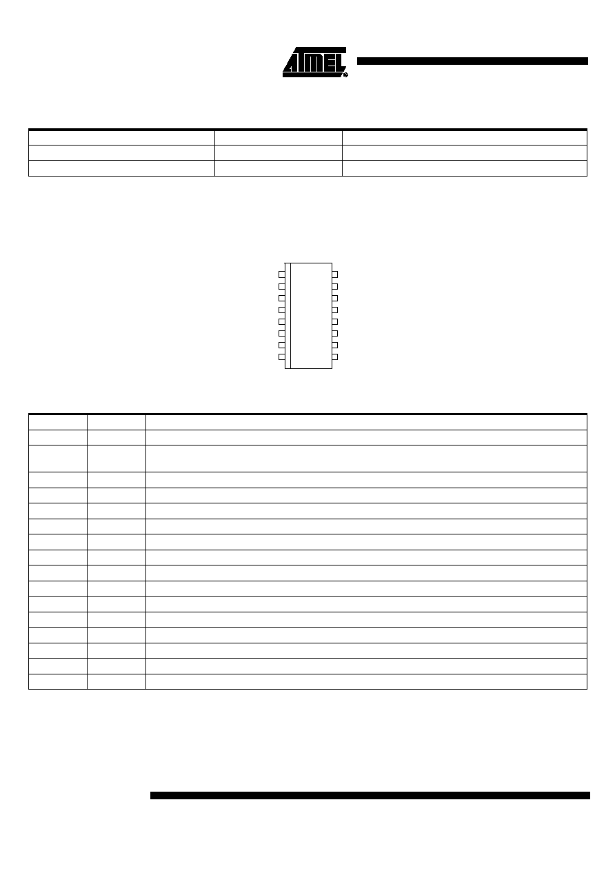
Pin Configuration
Figure 2.
Ordering Information
Extended Type Number
Package
Remarks
U3280M≠MFB
SSO16
Tube
U3280M≠MFBG3
SSO16
Taped and reeled
1
2
3
4
5
6
7
8
16
15
14
13
12
11
10
9
VBatt
VDD
SCL
NRST
SDA
VSS
n.c.
FC
Coil 2
Coil 1
n.c.
n.c.
n.c.
n.c.
NGAP
MOD
Pin Description
Pin
Symbol
Function
1
V
Batt
Power supply voltage input to connect a battery
2
V
DD
Power supply voltage for the
µ
C and EEPROM. At this pin a buffer capacitor (0.5... 10
µ
F) must be
connected to buffer the voltage during field supply and to block the VDD of the
m
C.
3
SCL
Serial clock line
4
NRST
Reset line bidirectional
5
SDA
Serial data line
6
V
SS
Circuit ground
7
n.c.
Not connected
8
FC
Field clock output of the front end clock extractor
9
MOD
Modulation input
10
NGAP
Gap and field detect output
11
n.c.
Not connected
12
n.c.
Not connected
13
n.c.
Not connected
14
n.c.
Not connected
15
Coil 1
Coil input 1. Pin to connect a resonant circuitry for communication and field supply
16
Coil 2
Coil input 2, see above

3 (17)
U3280M
Rev. A4, 11-Dec-01
Functional Description
The Transponder
Interface
The U3280M is a transponder interface IC which is able to operate microcontrollers
wireless and battery-independent. Wireless data communication and power supply are
handled via an electromagnetic field and the coil antenna of the transponder interface.
The U3280M consists of a rectifier stage for the antenna, a power management to han-
dle field and battery power supply, a damping modulator and a field-gap detection stage
for contactless data communication, further a field clock extraction and an EEPROM are
on the chip.
The internal rectifier stage rectifies the AC from the LC-resonant circuit at the coil inputs
and supplies the U3280M device and an additional microcontroller device with power. It
is also possible to supply the device via the VBatt input with DC from a battery. The
power management handles switching between battery supply (VBatt pin) and field sup-
ply automatically. It switches to field supply if a field is applied at the coil and it switches
back to battery if the field is removed. The voltage from the coil or the VBatt pin is output
at the VDD pin to supply the microcontroller or any other suited device. At the VDD pin a
capacitor must be connected to smooth and buffer the supply voltage. This capacitor is
also necessary to buffer the supply voltage during the communication (damping and
gaps in the field).
For communication, the chip contains a damping stage and a gap-detect circuitry. By
means of the damping stage the coil voltage can be modulated to transmit data via the
field. It can be controlled with the modulator input (MOD pin) via the microcontroller. The
gap-detection circuitry detects gaps in the field and outputs the gap/field signal at the
gap-detect output (Pin NGAP).
For the storage of data like keycodes, identifiers and configuration bits a 512-bit
EEPROM is available on the chip. It can be read and written by the microcontroller via
an I
2
C compatible two-wire serial interface.
The serial interface, the EEPROM and the microcontroller are supplied with the voltage
at the VDD pin. That means the microcontroller can read and write the EEPROM if the
supply voltage at VDD is in the operating range of the IC.
The U3280M has build in operating modes to support a wide range of applications.
These modes can be activated via the serial interface with special mode control bytes.
To support applications with battery supply only, the power management can be
switched off by software to disable the automatic switching to field supply.
An on-chip Biphase and Manchester modulator can be activated and controlled by the
serial interface. If this modulator is used it modulates the serial data stream at the serial
inputs SDA and SCL into a Biphase or Manchester coded signal for the damping stage.
Modulation
The transponder interface can modulate the magnetic field by its damping stage to
transmit data to a base station. It modulates the coil voltage by varying the coil's load.
The modulator can be controlled via the MOD pin. A high level ("1" ) increases the cur-
rent into the coil and damps the coil voltage. A low level ("0") decreases the current and
increases the coil voltage. The modulator generates a voltage stroke of about 2 V
pp
at
the coil. A high level at the MOD pin makes the maximum of the field energy available at
VDD. During a reset a high level at the MOD pin causes the optimum conditions for
starting the device and charging the capacitor at VDD after the field is applied at the coil.
Digital input to control the damping stage (MOD)
MOD = 0: coil not damped

4 (17)
U3280M
Rev. A4, 11-Dec-01
V
coil-peak
= VDD x
2 + V
CMS
= V
CU
MOD = 1: coil damped
V
coil-peak
= VDD x
2 = V
CD
V
CMS
= V
CID
: modulation voltage stroke @ coil inputs
Note:
If the automatic power management is disabled, the internal front end V
DD
is limited at
V
DDC
. In this case the value V
DDC
must be used in the above formula.
Field Clock
The field clock extractor of the interface makes the field clock available for the microcon-
troller. It can be used to supply timer inputs to synchronize modulation and
demodulation with the field clock.
Gap Detect
The transponder interface can also receive data. The base station modulates the data
with short gaps in the field. The gap-detection circuit detects these gaps in the magnetic
field and outputs the NGAP/field signal at the NGAP pin. A high level indicates that a
field is applied at the coil and a low level indicates a gap or that the field is off. The
microcontroller must demodulate the incoming data stream at one of its inputs.
U3280M Signals and Timing
Figure 3.
Modulation
Figure 4.
GAP and Modulation Timing
MOD
Coil inputs
V
CD
V
CU
V
CMS
t
FBS
t
BFS
Coil supply if automatically power management is enabled
Battery
supply
Battery supply
Coil inputs
NGAP
Field clock FC
Power management
1. edge used as wakeup signal
t
FGAP0
V
FDON
t
FGAP1
V
FDOFF
Gap detection and battery to field switching

5 (17)
U3280M
Rev. A4, 11-Dec-01
Digital output of the gap≠detection stage (NGAP)
NGAP = 0: gap detected / no field
V
COIL_peak
= V
FDoff
NGAP = 1: field detected
V
COIL-peak
= V
FDon
Note:
No amplifier is used in the gap-detection stage. A digital Schmitt trigger evaluates the
rectified and smoothed coil voltage.
Wake-up Signal
If a field is applied at the coil of the transponder interface the microcontroller can be
woken up with the wake signal at the NGAP pin. For that purpose the NGAP pin must be
connected to an interrupt input of the microcontroller. A high level at the NGAP output
indicates an applied field and can be used as wake signal for the microcontroller via an
interrupt. The wake signal is generated if the power management switches to field sup-
ply. The field-detection stage of the power management has lowpass characteristics to
avoid generating of wake signals and unnecessary switching between battery and field
supply in case of interferences at the coil inputs.
Power Supply
The U3280M has a power management that handles two power supply sources. Nor-
mally the IC is supplied by a battery at the VBatt pin. If a magnetic field is applied at the
LC-resonant circuit of the device the field detection circuit switches automatically from
VBatt to field supply.
The VDD pin is used to connect a capacitor to smooth the voltage from the rectifier and
to buffer the power while the field is modulated by gaps and damping. The EEPROM
and the connected controller always operate with the voltage at the VDD pin.
Note:
During field supply the maximum energy from the field is used if a high level is applied at
the MOD input!
Automatic Power
Management
There are different conditions to switch from the battery to field and back from field to
the battery.
The power management switches from battery to field if the rectified voltage (Vcoil) from
the coil inputs becomes higher than the field-on-detection voltage (V
FDon
), even if no
battery voltage is available (0 < V
Batt
< 1.8 V). It switches back to battery if the coil volt-
age becomes lower than the field-off-detection voltage (V
FDoff
).
The field detection stage of the power management has lowpass characteristics to sup-
press noise. An applied field needs a time delay t
BFS
(battery-to-field switch delay) to
change the power supply. If the field is removed from the coil, the power management
will generate a reset that can be connected to the microcontroller.
Figure 5. Switch conditions for the power management
Note:
The rectified supply voltage from the coil is limited to V
DDC
(2.9 V). During field supply
the battery is switched off and V
DD
changes to V
DDC
.
Battery
supply
Field
supply
V
Coil
> V
FDon
for t > t
BFS
V
Coil
< V
FDon
for t > t
BFS
(V
Batt
)