
1
Features
∑
All Functions and Channel Selections are Controlled by Serial Bus
RF Part
∑
All Oscillators and PLL Integrated
∑
IF Converter
∑
FM Demodulator
∑
RSSI
Low Frequency Part
∑
Asymmetrical Input of Microphone Amplifier
∑
Asymmetrical Output of Earpiece Amplifier
∑
Compander
∑
Power Supply Management
∑
Serial Bus
Application
∑
CT0 Standard
∑
Narrowband Voice and Data Transmitting/Receiving Systems
Description
The programmable single-chip multichannel cordless phone IC includes all necessary
low frequency parts such as microphone- and earphone amplifier, compander, power-
supply management as well as all RF parts such as IF converter, FM demodulator,
RSSI, oscillators and PLL. Several gains and mutes in transmit and receive direction
are controlled by the serial bus. The compander can be bypassed.
Single-chip
Cordless
Telephone IC
U3600BM
Preliminary
Rev. 4516C≠CT0≠08/02
2
U3600BM
4516C≠CT0≠08/02
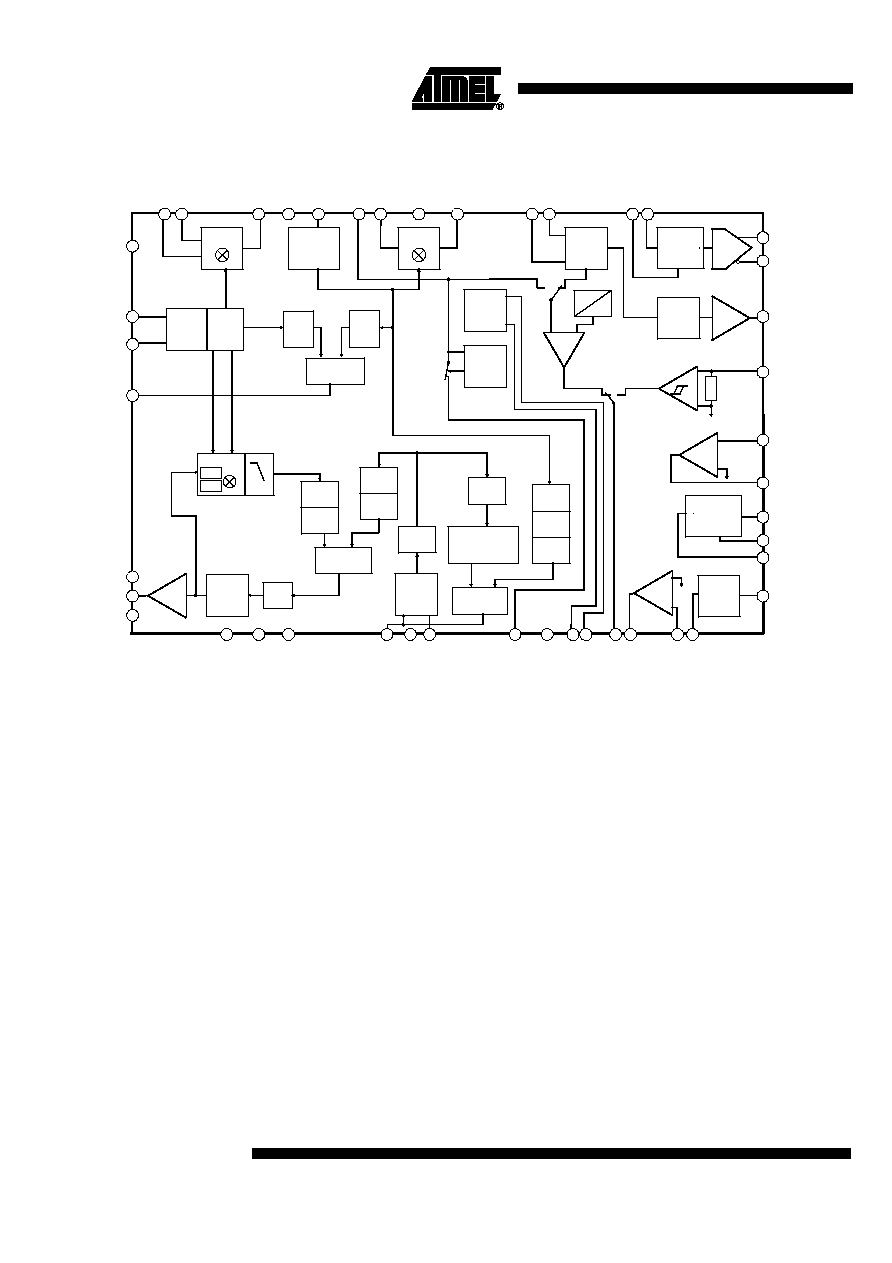
Figure 1. Block Diagram
Mixer1
VCO3
:2
sin
cos
fLO
MixerT
+45
-45
Crystal
Mixer2
IF
RSSI
:N
:K
Phase
fLO
fRef3
f LO
VCO2
Loop
:D2
:M12
:D1
:2
VCO1
:D3
fRef1
:2
:10
:M
Serial
Bus
Bias
Bat low
Detector
-
+
D
A
MUXDA
1.5V
-
+
Expander
Demo-
Ear
-
+
Mic
VRMIC
Compressor
Limiter
Spl 1.5V
DATRX
:M12
MIX1IN2
MIX1IN1
MIX1O
OSCGND
XCK
VAF
MIX2O
MIX2GND
MIX2IN
IFIN1
IFIN2
ETC
EXIN
RECO1
RECO2
RXO
DAIN
MIC
MICO
COIN
CTC
COUT
LIMIN
TXO
OPIN
OPOUT
DACO
D C
VSS
VDD
MODIN
LFGND
MLF
VRF
VBIAS
AGND
RFOVB
RFO
RFOGND
PCLO
LO1
LO2
GNDLO
Oscillator
Comparator
(3)
(2)
(1)
Filter
Phase
Comparator
Phase
Comparator
f Ref2
-
+
1
1
5
6
7
8
9
10
11
12
13
14
15 16
17
18
2
3
4
19
20
21
22
23
24
25
26
27
28
29
30
31
32
33
34
35
36
37
38
39
40
41
42
43
44
fMod
dulator
Amp
Amp
Amp
(1): PLL1: Modulator PLL
(2): PLL2: Mixer PLL
(3): PLL3: Local oscillator (LO) PLL
3
U3600BM
4516C≠CT0≠08/02
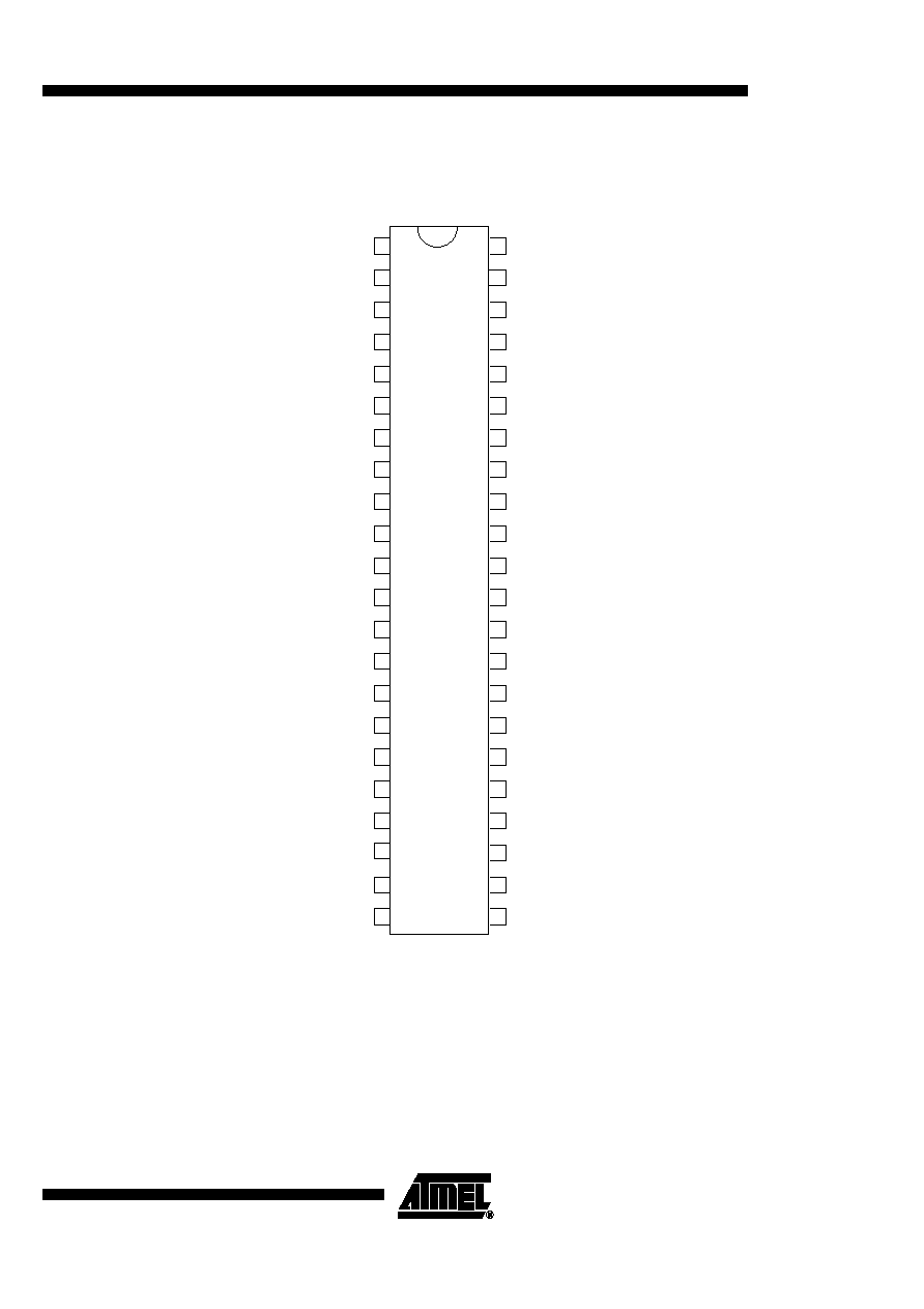
Pin Configuration
Figure 2. Pinning SSO44
1
2
3
4
5
6
7
8
9
10
11
12
13
14
15
16
17
18
19
20
21
22
44
43
42
41
40
39
38
37
36
35
34
33
32
31
30
29
28
27
26
25
24
23
LO1
LO2
GNDLO
MIX1IN1
MIX1O
OSCGND
XCK
VAF
MIX2O
MIX2IN
IFIN1
IFIN2
ETC
EXIN
RECO1
RECO2
RXO
DAIN
MIC
MICO
RFOGND
RFO
RFOVB
AGND
VBIAS
VRF
LFGND
MODIN
VSS
DACO
OPOUT
OPIN
TXO
LIMIN
COUT
CTC
COIN
C
PCLO
MIX1IN2
MIX2GND
D
VDD
MLF
4
U3600BM
4516C≠CT0≠08/02
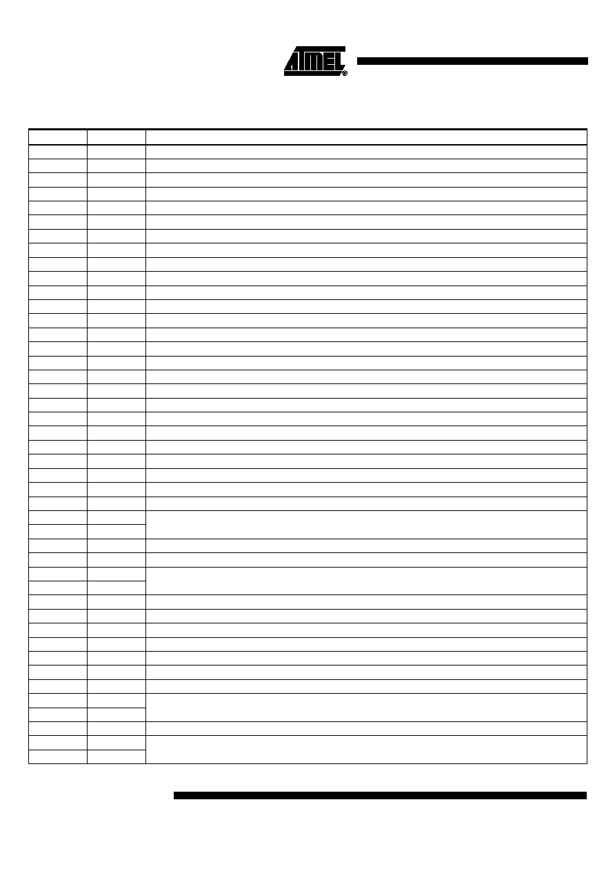
Pin Description
Pin
Symbol
Function
1
PCLO
Phase comparator local oscillator
2
RFOGND
RF transmit output ground
3
RFO
RF transmit output
4
RFOVB
Power supply input of RF transmit output buffer
5
AGND
Analog ground for RF part
6
VBIAS
Decoupling capacitor of current reference
7
VRF
Supply voltage for RF part
8
MLF
Modulator loop filter
9
LFGND
Modulator loop filter ground
10
MODIN
Modulator input
11
VDD
Supply voltage output for peripherals and internal supply of digital part
12
VSS
Ground for LF analog and digital
13
D
Data input of serial bus
14
C
Clock input of serial bus
15
DACO
D/A and data comparator output
16
OPOUT
Operational amplifier output
17
OPIN
Operational amplifier input (inverting)
18
TXO
Output of limiter amplifier
19
LIMIN
Limiter input
20
COUT
Compressor output
21
CTC
Compressor time constant control analog output
22
COIN
Compressor input
23
MICO
Microphone amplifier output
24
MIC
Inverting input of microphone amplifier
25
DAIN
Data comparator input
26
RXO
Output of demodulator
27
RECO2
Symmetrical output of receive amplifier
28
RECO1
29
EXIN
Expander input
30
ETC
Expander time constant control analog output
31
IFIN2
Symmetrical input of IF amplifier
32
IFIN1
33
MIX2IN
Input of Mixer2
34
MIX2GND
IF amplifier and Mixer2 ground
35
MIX2O
Mixer2 output
36
VAF
Supply voltage for AF/IF parts
37
XCK
Crystal oscillator input 11.15 MHz
38
OSCGND
Oscillator ground
39
MIX1O
Output of Mixer1
40
MIX1IN1
Symmetrical input of MIxer1
41
MIX1IN2
42
GNDLO
Ground of LO
43
LO2
Tank elements for LO are connected to these pins
44
LO1

5
U3600BM
4516C≠CT0≠08/02
System Description
Radio frequency IC for analog cordless telephone application in 26/50 MHz band (CTO
standard). The IC performs full duplex communication. The transmitting and receiving
frequency are depending on whether the IC is used in the handset or in the base station.
Frequency converter comprise an FM transmitter with switchable output power and first
receiver mixer in the same unit. A two-wire bus interface can be used for the frequency
control as well as for switching the transmitter power amplifier and the receiver. Fine
frequency adjust of reference quartz oscillator is programmable.
The receive part is designed for a double conversion architecture. The incoming radio
frequency signal will be filtered and amplified before reaching the first mixer. At this
stage the RF signal will be converted down to the first intermediate frequency
(10.7 MHz) by using a crystal oscillator (LO1).
The transmit part contains two PLL controlled VCOs. The frequency modulation is
accomplished by super-posing the incoming audio signal on the PLL control voltage.
Final frequency is a product of mixing VCO1 with first local oscillator of receiver part
(VCO3). The FM modulated carrier is amplified by externals power amplifier before
entering the output filter and the antenna connector.
Adjustments for VCO1
and VCO2
To be able to use a wide frequency range for the VCOs (i.e., VCO2 26.3 MHz to
49.9 MHz) the two internal VCOs (VCO1 and VCO2, i.e., the VCOs of the transmit part)
have a rough adjust and a fine adjust to increase the frequency range given by the
phase comparator.
The rough adjusts for these VCOs are correlated with the country setting. For every
country there are two sets of VCO rough adjust settings, one for the base and one for
the handset. See tables at channels frequencies and dividers.
To compensate the variation in production there is a fine adjust for each of the VCOs.
The fine adjusts of the internal VCOs could be set manually (for test purposes) or set by
the automatic mode. Theoretically the sign of the changing (increase/ decrease when
the voltage of the phase comparator is to high) is selectable, but we need value 1 () in all
cases.
Setting VCO1 (VCO2) under normal conditions:
EAFA1 (EAFA2) = 1, automatic fine adjust VCO1(VCO2) enabled
SAFA1 (SAFA2) = 1, sign of auto fine adjustment of VCO1 (VCO2) = 1.
Adjustment for VCO3
In order to increase the adjustment range of VCO3 with fixed external tank elements
and/or for "band switching", especially for US frequencies, VCO3 has programmable
capacitors inside. These capacitors can be added by serial bus (FA3 [4:0]) between LO1
and LO2. There are 31 steps available, every step adding a capacitor of 0.5pF.
Speed-up of the Loop
Filter of PLL1
("Modulator PLL")
To have a fast locking time for the modulator loop there is a precharge and a speed-up
mode for the external loop filter.
During receive mode (VCO3 enabled, VCO1 disabled) the modulator loop filter is
precharged to about half of the internally regulated 2.5 V charge-pump voltage.
During the first 30 ms after enabling VCO1 the modulator phase comparator is in speed-
up mode. In this mode the current of the pase comparator which charges the loop filter
is much larger than in normal mode. Additionally to the automatically switched 30 ms
speed-up mode, the speed-up can be activated for any time by setting the bit SU1.