
1
Features
∑
DC Characteristic Adjustable
∑
Transmit and Receive Gain Adjustable
∑
Symmetrical Input of Microphone Amplifier
∑
Anti-clipping in Transmit Direction
∑
Automatic Line-loss Compensation
∑
Built-in Ear Protection
∑
DTMF and MUTE Input
∑
Adjustable Sidetone Suppression Independent of Sending and Receiving
Amplification
∑
Integrated Amplifier for Loudhearing Operation
∑
Anti-clipping for Loudspeaker Amplifier
∑
Improved Acoustical Feedback Suppression
∑
Selectable Line Impedance
∑
Voice Switch
∑
Supply Voltages for All Functional Blocks of a Subscriber Set
∑
Operation Possible from 10-mA Line Current
∑
Filters Against EMI on Critical I/O
Benefits
∑
Complete System Integration of Analog Signal Processing on One Chip
∑
Very Few External Components
∑
Less Components for EMI protection
Applications
∑
Feature Phones
∑
Answering Machines
∑
Fax Machines
∑
Speaker Phones
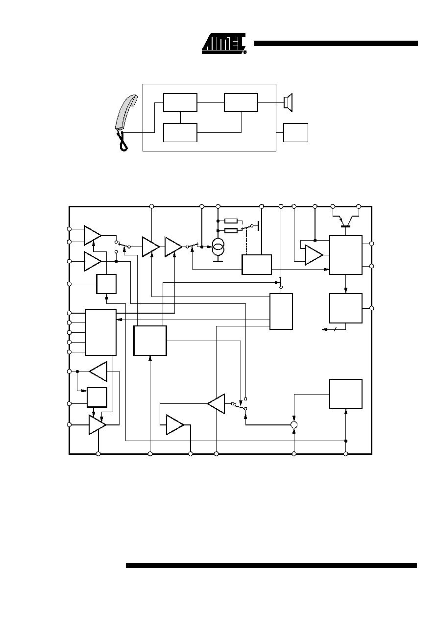
Description
The telephone circuit U4089B-P is a linear integrated circuit for use in feature phones,
answering machines and fax machines. It contains the speech circuit, sidetone
equivalent and ear protection rectifiers. The circuit is line-powered and contains all
components necessary for the amplification of signals and adaptation to the line.
An integrated voice switch with loudspeaker amplifier enables loudhearing or hands-
free operation. With an anti-feedback function, acoustical feedback during loud-
hearing can be reduced significantly. The generated supply voltage is suitable for a
wide range of peripheral circuits.
Electrostatic sensitive device.
Observe precautions for handling.
Monolithic
Integrated
Feature Phone
Circuit
U4089B-P
Rev. 4518A≠CORD≠05/02
2
U4089B-P
4518A≠CORD≠05/02
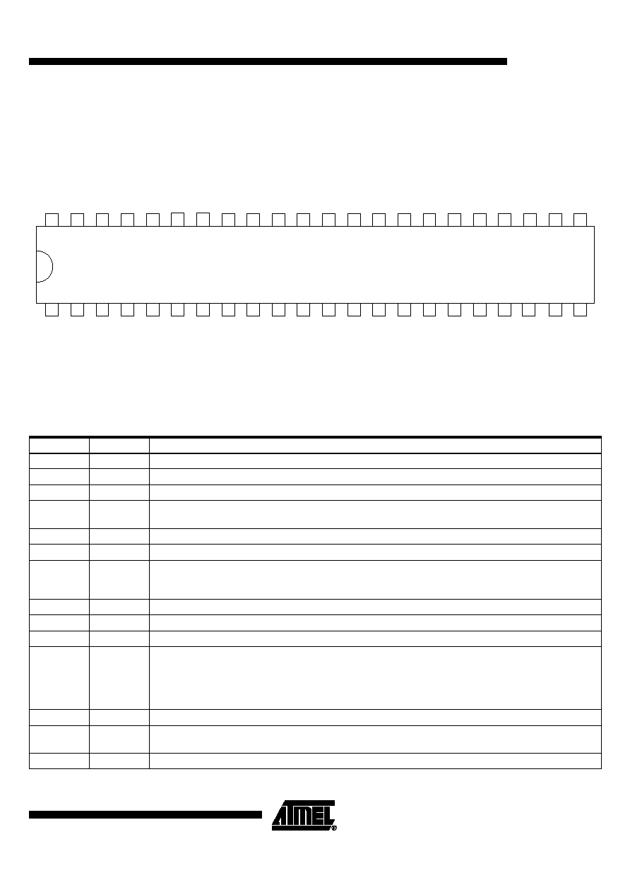
Figure 1. Simple Block Diagram
Figure 2. Block Diagram
Speech
circuit
Audio
amplifier
Voice
switch
Dialer
Acoustical
feedback
suppression
control
27
26
29
28
25
MIC
4
3
1
TX
ACL
41
SACL
11
21
Transmit
mute
control
23
TXA
AGA
control
R-
attenuation
Current
supply
Power
supply
13
10
9
6
30
7
32
44
Supply
24
22
39
40
36
42
MIC1
MIC2
DTMF
TTXA
INLDR
INLDT
TLDR
TLDT
ATAFS
SAO
TSACL
SAI
GSA
MUTX
RECO
GR
STI
RECIN
V
L
STO
GT
AGA IND
SENSE V
B
V
MP
I
REF
GND
V
M
600
900
20
IMPSEL
Impedance
control
31
8
33
3
U4089B-P
4518A≠CORD≠05/02
Pin Configuration
Figure 3. Pinning SSO44
1
2
3
4
5
6
7
8
9
10
11
12
13
14
15
16
17
18
19
20
21
22
44
43
42
41
40
39
38
37
36
35
34
33
32
31
30
29
28
27
26
25
24
23
IR
E
F
AGA
TL
DR
TL
DT
IN
L
D
R
IN
L
D
T
VM
STO
ATAF
S
NC
NC
STI
MUT
X
SAI
RECO
NC
NC
TTXA
GR
RECI
N
NC
GT
DT
M
F
NC
MI
C2
MI
C1
NC
IN
D
VL
GN
D
SENSE
VB
SAO
NC
VM
P
NC
NC
NC
NC
NC
NC
I
M
PSE
L
TSACL
GSA
Pin Description
Pin
Symbol
Function
1
DTMF
Input for DTMF signals. Also used for the answering machine and hands-free input.
3
MIC 2
Non-inverting input of microphone amplifier.
4
MIC 1
Inverting input of microphone amplifier.
6
IND
The internal equivalent inductance of the circuit is proportional to the value of the capacitor at this pin.
A resistor connected to ground may be used to reduce the DC line voltage.
7
V
L
Line voltage.
8
GND
Reference point for DC and AC output signals.
9
SENSE
A small resistor (fixed) connected from this pin to V
L
sets the slope of the DC characteristic and also
affects the line-length equalization characteristics as well as the line current at which the loudspeaker
amplifier is switched on.
10
V
B
Unregulated supply voltage for peripheral circuits (voice switch); limited to typically 7 V.
11
SAO
Output of loudspeaker amplifier.
13
V
MP
Regulated supply voltage 3.3 V for peripheral circuits. The maximum output current is 2 mA.
20
IMPSEL
Control input for selection of line impedance
1) 600
2) 900
3) Mute of second transmit stage (TXA); also used for indication of external supply (answering machine);
last chosen impedance is stored.
21
TSACL
Time constant of anti-clipping of speaker amplifier.
22
GSA
Current input for setting the gain of the speaker amplifier. Adjustment characteristic is logarithmical.
For RGSA > 2 M
,
the
speaker amplifier is switched off.
23
SA I
Speaker amplifier input (for loudspeaker, tone ringer and hands-free use).
Note:
Filters against electromagnetic interference (EMI) are located at the Pins MIC1, MIC2, RECIN and STI.

4
U4089B-P
4518A≠CORD≠05/02
24
MUTX
Three-state input of transmit mute:
1) Speech condition; inputs MIC1/MIC2 active.
2) DTMF condition; input DTMF active. A part of the input signal is passed to the receiving amplifier as
a confidence signal during dialing.
3) Input DTMF used for answering machine and hands-free use; receive branch is not affected.
25
ATAFS
Attenuation of acoustical feedback suppression. Maximum attenuation of AFS circuit is set by a resistor
at this pin. Without the resistor, AFS is switched off.
26
INLDT
Input of transmit level detector.
27
INLDR
Input of receive level detector.
28
TLDT
Time constant of transmit level detector.
29
TLDR
Time constant of receive level detector.
30
AGA
Automatic gain adjustment with line current. A resistor connected from this pin to GND sets the starting
point. Maximum gain change is 6 dB.
31
IREF
Internal reference current generation; RREF = 62 k
; IREF = 20 µA
32
STO
Side-tone reduction output. Output resistance is approximately 300
. Maximum load impedance is
10 k
.
33
V
M
Reference node for microphone-earphone and loudspeaker amplifier. Supply for electret microphone
(IM
300 mA).
36
STI
Input for side-tone network.
39
RECO
Output of receiving amplifier.
40
G
R
A resistor connected from this pin to GND sets the receiving amplification of the circuit; amplifier RA1
can be muted by applying V
MP
to G
R
.
41
TTXA
Time constant of anti-clipping in transmit path.
42
RECIN
Input of receiving path; input impedance is typically 80 k
.
44
G
T
A resistor from this pin to GND sets the amplification of microphone and DTMF signals; the input
amplifier can be muted by applying V
MP
to G
T
.
Pin Description
Pin
Symbol
Function
Note:
Filters against electromagnetic interference (EMI) are located at the Pins MIC1, MIC2, RECIN and STI.
5
U4089B-P
4518A≠CORD≠05/02
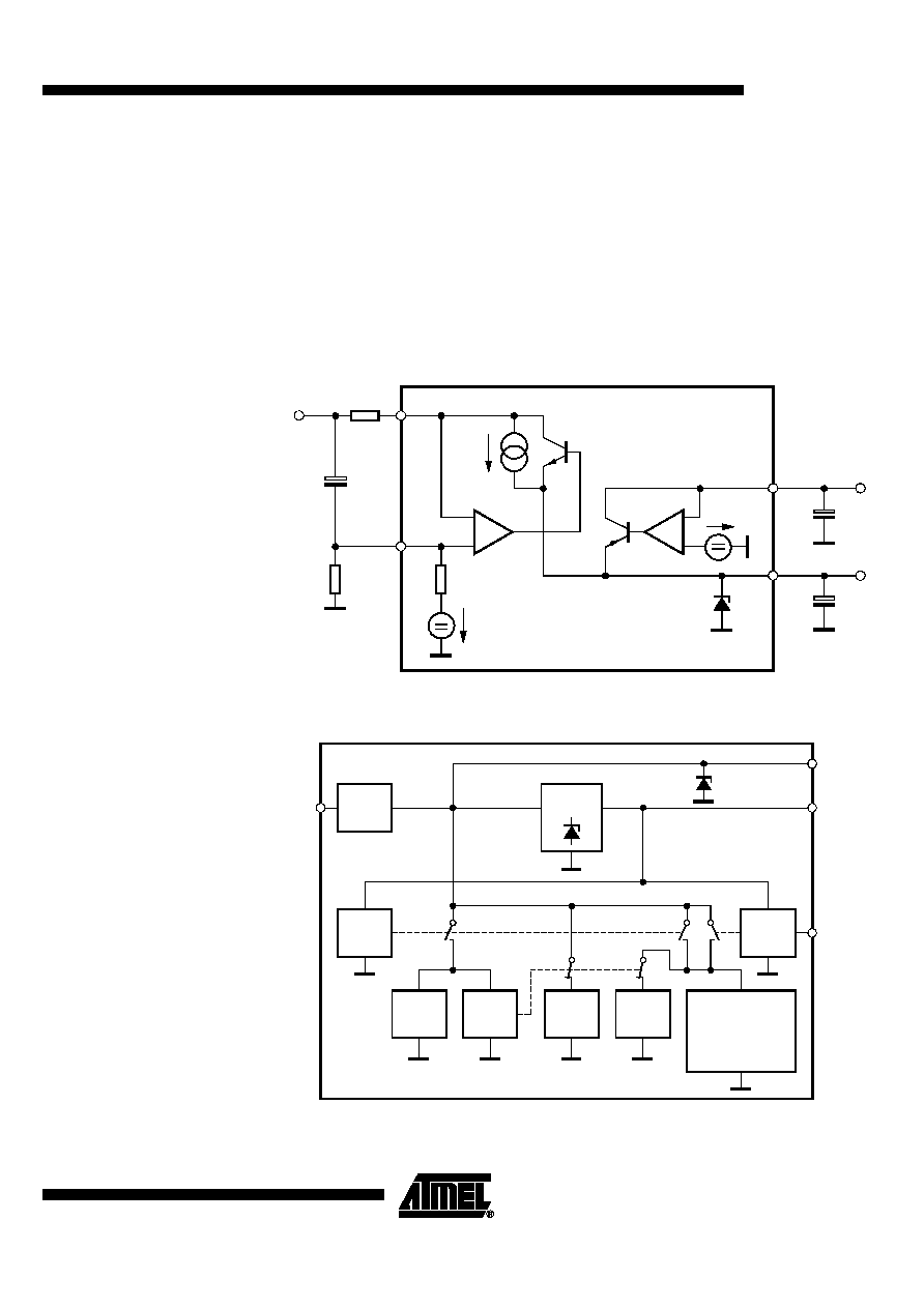
DC Line Interface and
Supply-voltage
Generation
The DC line interface consists of an electronic inductance and an output stage which
charges the capacitor at V
B
. The value of the equivalent inductance is given by:
L = R
SENSE
◊
C
IND
◊
(R
DC
◊
R
30
) / (R
DC
+ R
30
)
In order to improve the supply during worst-case operating conditions, the PNP current
source (I
BOPT
)
supplies an extra amount of current to the supply voltages when the NPN
in parallel is unable to conduct current.
The U4089B-P contains a series regulator which provides a supply voltage V
MP
of 3.3 V
at 2 mA suitable for a microprocessor.
Figure 4. DC Line Interface with Electronic Inductance and Generation of Regulated
and Unregulated Supply
Figure 5. Functional Blocks for Power Supply
-
+
I
BOPT
< 5 mA
30 k
R
30
V
OFFS
SENSE
IND
R
SENSE
10
10
µ
F
R
DC
C
IND
V
L
-
+
3.3 V
7 V
V
MP
V
B
3.3 V/
2 mA
47
µ
F
220
µ
F
7V
V
B
MIC, DTMF
AGA, RA
TX MUTE
MUT REC, STBAL
RECATT
AFS
SAL, SA
SACL
OFFSA
COMP
TXA
TXACL
LIDET
Voltage
regulator
Power
supply
V
L
V
LON
V
MP
IMPED
CONTR
IMPSEL
ES