U4090B
Rev. C2, 07-Mar-01
1 (31)
Monolithic Integrated Feature Phone Circuit
Description
The
µ
c-controlled telephone circuit U4090B is a linear
integrated circuit for use in feature phones, answering
machines and fax machines. It contains the speech circuit,
tone ringer interface with DC/DC converter, sidetone
equivalent and ear protection rectifiers. The circuit is line
powered and contains all components necessary for
amplification of signals and adaptation to the line.
An integrated voice switch with loudspeaker amplifier
allows loudhearing or hands-free operation. With an
anti-feedback function, acoustical feedback during
loudhearing can be reduced significantly. The generated
supply voltage is suitable for a wide range of peripheral
circuits.
Features
D DC characteristic adjustable
D Transmit and receive gain adjustable
D Symmetrical input of microphone amplifier
D Anti-clipping in transmit direction
D Automatic line-loss compensation
D Symmetrical output of earpiece amplifier
D Built-in ear protection
D DTMF and MUTE input
D Adjustable sidetone suppression independent
of sending and receiving amplification
D Speech circuit with two sidetone networks
D Built-in line detection circuit
D Integrated amplifier for loudhearing operation
D Anti-clipping for loudspeaker amplifier
D Improved acoustical feedback suppression
D Power down
D Voice switch
D Tone ringer interface with dc/dc converter
D Zero crossing detection
D Common speaker for loudhearing and tone ringer
D Supply voltages for all functional blocks of a
subscriber set
D Integrated transistor for short circuiting the line
voltage
D Answering machine interface
D Operation possible from-10 mA line currents
Benefits
D Savings of one piezo-electric transducer
D Complete system integration of analog signal proces-
sing on one chip
D Very few external components
Applications
Feature phone, answering machine, fax machine, speaker
phone
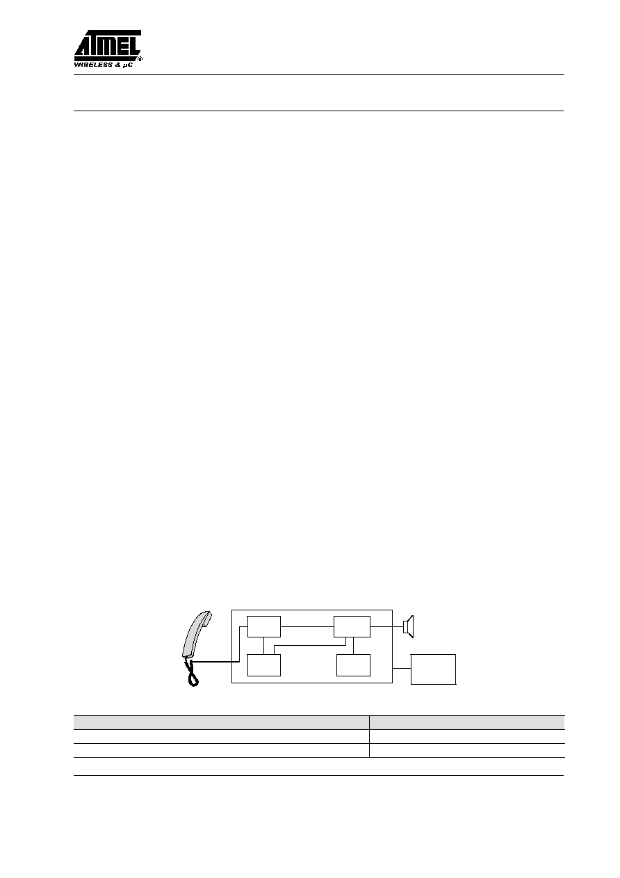
Block Diagram
MC with
EEPROM/
DTMF
Audio
amplifier
Speech
circuit
Voice
switch
Tone
ringer
Loudhearing
and
Tone ringing
94 8741
Ordering Information
Extended Type Number
Package
Remarks
U4090B-NFN
SSO44
U4090B-NFNG3
SSO44
Taped and reeled
U4090B
Rev. C2, 07-Mar-01
2 (31)
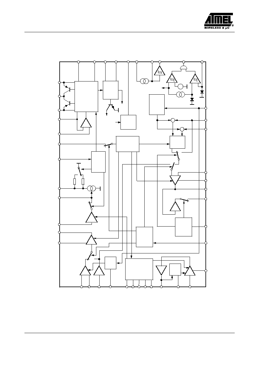
Detailed Block Diagram
GT
MICO
TXIN
ST
O
V
L
IMPSEL
AGA
IND
SENSE
V
B
V
MP
V
MPS
V
M
GND
PD
I REF
LIDET
V
RING
C
OSC
SW
OUT
RFDO
THA
RECIN
STIS
STIL
RAC
GR
RECO2
RECO1
MUTR
MUTX
GSA
MIC1
MIC2
DTMF
TTXA
INLDR
TLDR
A
T
AFS
SAO
TSACL
SAI
MIC
TX
ACL
Acoustical
feedback
suppression
control
T
ransmit
mute
control
SACL
Mute
receive
control
Impedance
control
Power
supply
Current
supply
I Supply
Line
detect
AGA
control
I L
Receive
attenuation
V
L
+
≠
≠
+
V
MP
ST
BAL
TXA
94 8064
Q
S
INLDT
TLDT
≠1
600
W
900
W
+
+
≠
≠
1
2
6
4
12
5
7
8
9
11
10
3
16
15
23
22
24
25
26
20
27
21
19
14
13
28
31
30
29
38
37
36
33
35
34
32
42
39
41
40
43
44
17
18
DTMF
RA1
RA2
SA
SAI
Figure 1. Detailed block diagram
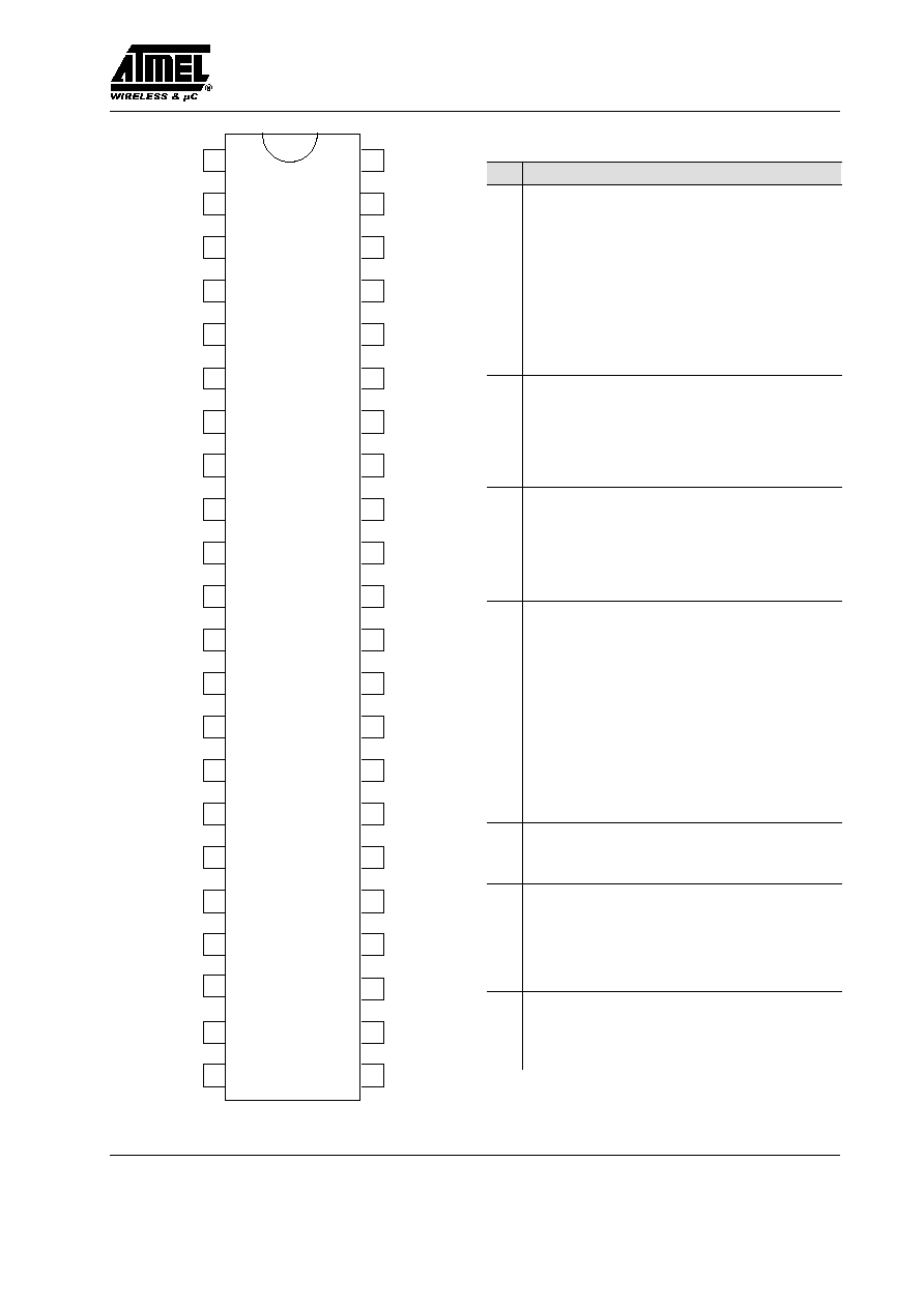
U4090B
Rev. C2, 07-Mar-01
3 (31)
1
2
3
4
5
6
7
8
9
10
11
12
13
14
15
16
17
18
19
20
21
22
44
43
42
41
40
39
38
37
36
35
34
33
32
31
30
29
28
27
26
25
24
23
TXIN
RECIN
TTXA
RECO1
RAC
STIL
STIS
RECO2
MUTR
STO
IREF
AGA
TLDR
TLDT
INLDR
INLDT
ATAFS
MUTX
SAI
GSA
DTMF
MICO
MIC2
MIC1
PD
IND
GND
SENSE
SAO
SWOUT
COSC
VRING
THA
RFDO
LIDET
IMPSEL
TSACL
U4090B
GT
VL
VB
VMPS
GR
VM
94 7905 e
VMP
Pin Description
Pin
Symbol
Function
1
G
T
A resistor from this pin to GND sets the
amplification of microphone and DTMF
signals,theinputamplifiercanbemuted by
applying VMP to G
T
.
2
DTMF
Input for DTMF signals,
also used for the answering machine
and hands-free input
3
MICO
Output of microphone preamplifier
4
MIC 2
Non-inverting input of microphone
amplifier
5
MIC 1
Inverting input of microphone
amplifier
6
PD
Active high input for reducing the
current consumption of the circuit,
simultaneously V
L
is shorted by an
internal switch
7
IND
The internal equivalent inductance of
the circuit is proportional to the value
of the capacitor at this pin,
a resistor connected to ground may be
used to reduce the dc line voltage
8
V
L
Line voltage
9
GND
Reference point for dc- and ac-output
signals
10
SENSE
A small resistor (fixed) connected
from this pin to V
L
sets the slope of
the dc characteristic and also effects
the line-lengthequalization
characteristics and the line current at
which the loudspeaker amplifier is
switched on
11
V
B
Unregulated supply voltage for
peripheral circuits (voice switch),
limited to typically 7 V
12
SAO
Output of loudspeaker amplifier
13
V
MPS
Unregulated supply voltage for
µ
C,
limited to 6.3 V
14
V
MP
Regulated supply voltage 3.3 V for
peripheral circuits (especially
microprocessors),
minimum output current: 2 mA
(ringing)
4 mA (speech mode)
15
SWOUT
Output for driving external switching
transistor
16
COSC
40-kHz oscillator for ringing power
converter
U4090B
Rev. C2, 07-Mar-01
4 (31)
Pin
Symbol
Function
17
V
RING
Input for ringing signal protected by
internal zener diode
18
THA
Threshold adjustment for ringing
frequency detector
19
RFDO
Output of ringing frequency detector
20
LIDET
Line detect; output is low when the
line current is more than 15 mA
21
IMP-
SEL
Control input for selection of line
impedance
1. 600
2. 900
3. Mute of second transmit stage
(TXA); also used for indication of
external supply (answering machine);
last chosen impedance is stored
22
TSACL
Time constant of anti-clipping of
speaker amplifier
23
GSA
Current input for setting the gain of
the speaker amplifier,
adjustment characteristic is
logarithmical,
or RGSA > 2 M
,
the
speaker
amplifier is switched off
24
SA I
Speaker amplifier input (for
loudspeaker, tone ringer and
hands-free use)
25
MUTX
Three-state input of transmit mute:
1) Speech condition; inputs MIC1 /
MIC2 active
2) DTMF condition; input DTMF
active
a part of the input signal is
passed to the receiving amplifier
as a confidence signal during
dialing
3) Input DTMF used for answering
machine and hands-free use;
receive branch not affected
26
ATAFS
Attenuation of acoustical feedback
suppression,
maximum attenuation of AFS circuit
is set by a resistor at this pin,
without the resistor, AFS is switched
off
27
INLDT
Input of transmit level detector
28
INLDR
Input of receive level detector
Pin
Symbol
Function
29
TLDT
Time constant of transmit level
detector
30
TLDR
Time constant of receive level
detector
31
AGA
Automatic gain adjustment with line
current
a resistor connected from this pin to
GND sets the starting point
max. gain change: 6 dB.
32
IREF
Internal reference current generation;
RREF = 62 k
; IREF = 20
µ
A
33
STO
Sidetone reduction output
output resistance approx.: 300
,
maximum load impedance: 10 k
.
34
V
M
Reference node for microphone-
earphone and loudspeaker amplifier,
supply for electret microphone
(IM
700
mA)
35
MUTR
Three-state mute input
1. Normal operation
2. Mute of ear piece
3. Mute of RECIN signal
Condition of earpiece mute is stored
36
RECO 2 Inverting output of receiving
amplifier
37
STI S
Input for sidetone network (short
loop) or for answering machine
38
STI L
Input for sidetone network (long
loop)
39
RAC
Input of receiving amplifier for ac
coupling in feedback path
40
RECO 1 Output of receiving amplifier
41
G
R
A resistor connected from this pin to
GNDsetsthereceivingamplification of
the circuit; amplifier RA1 can be
muted by applying VMP to GR
42
TTXA
Time constant of anti-clipping in
transmit path
43
RECIN
Input of receiving path; input
impedance is typically 80 k
W
44
TXIN
Input of intermediate transmit stage,
input resistance is typically 20 k
U4090B
Rev. C2, 07-Mar-01
5 (31)
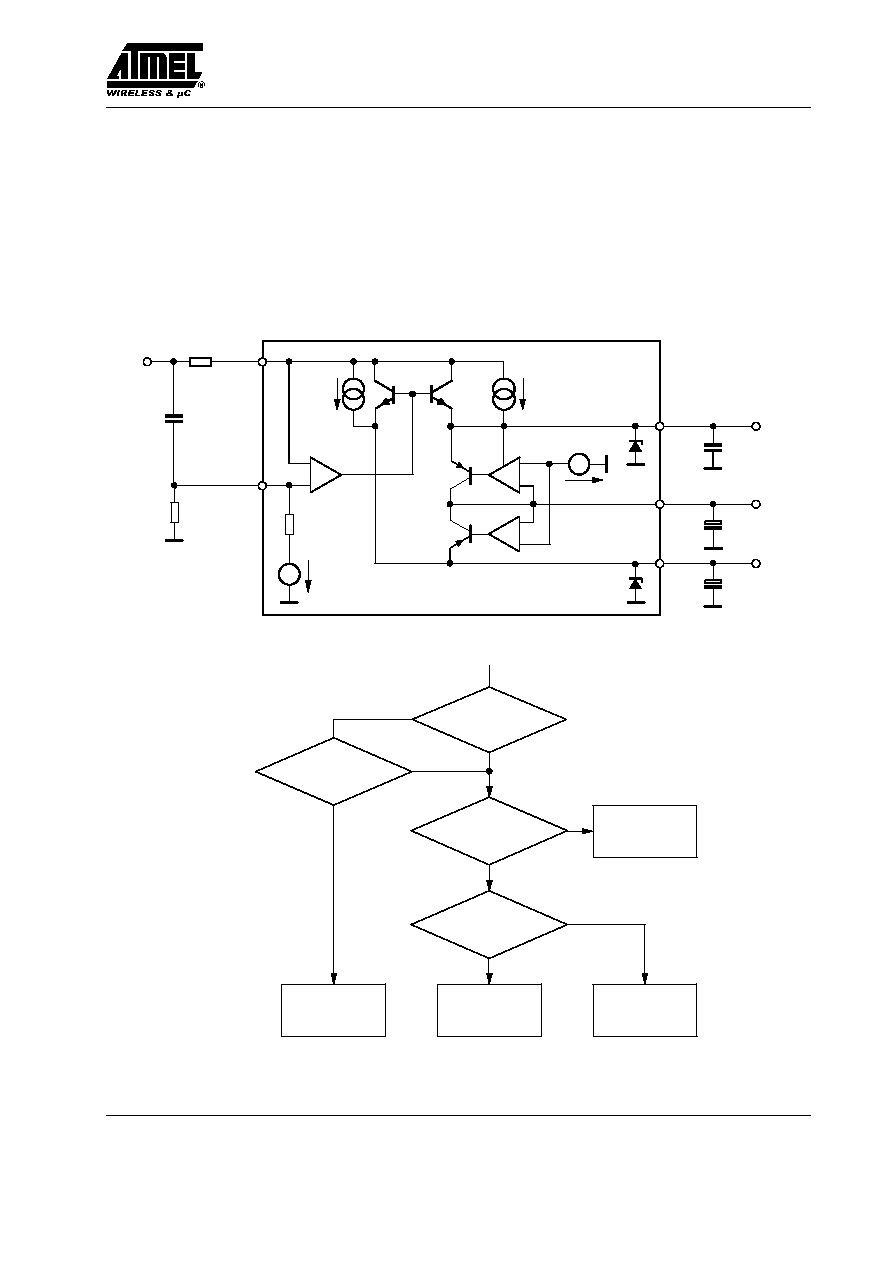
DC Line Interface and Supply-Voltage Generation
The DC line interface consists of an electronic inductance
and a dual-port output stage which charges the capacitors
at V
MPS
and V
B
. The value of the equivalent inductance
is given by:
L = R
SENSE
C
IND
((R
DC
R
30
) / (R
DC
+ R
30
))
In order to improve the supply during worst-case operat-
ing conditions, two PNP current sources - I
BOPT
and
I
MPSOPT
- hand an extra amount of current to the supply
voltages when the NPNs in parallel are unable to conduct
current.
A flowchart for the control of the current sources
(figure 3) shows how a priority for supply V
MPS
is
achieved.
≠
+
+
≠
+
≠
V
L
10
W SENSE
R
SENSE
C
IND
10 F
I
BOPT
< 5 mA
I
MPSOPT
30 k
W
V
OFFS
6.3 V
3.3 V
V
MPS
V
MP
V
B
470 F
47 F
220 F
3.3 V/
2 mA
7.0 V
94 8047
m
m
m
m
=
=
< 5 mA
IND
R
DC
R
30
Figure 2. DC line interface with electronic inductance and generation of a regulated and an unregulated supply
VSENSE≠VB>200 mV
VSENSE≠VMPS>200 mV
VB < 6.3 V
Charge CB
(IBOPT)
Charge CMPS
(IMPSOPT)
VMPS < 6.3 V
IBOPT = 0
Reduce IBOPT
(IMPSOPT = 0)
Y
N
Y
IMPSOPT = 0
N
N
N
Y
Y
94 8058
Figure 3. Supply capacitors CMPS and CB are charged with priority on CMPS