1
Features
∑
FM Double-conversion System
∑
Integrated Second IF Filter with Software-controlled Bandwidth
∑
Completely Integrated FM Demodulator
∑
Soft Mute and Multipath Noise Cancellation
∑
Receiving Condition Analyzer
∑
AM Up/Down-conversion System
∑
AM Preamplifier with AGC and Stereo Capability
∑
3-wire Bus Controlled
∑
Search Stop Signal Generation for AM and FM
∑
Automatic Alignment Possible
Electrostatic sensitive device.
Observe precautions for handling.
Description
The U4255BM-M is a highly integrated AM/FM front-end circuit manufactured using
Atmel's advanced BICMOS technology. It represents a complete, automatically adjust-
able AM/FM front end, containing a double-conversion system for FM and an
up/down-conversion receiver for AM with IF1 = 10.7 MHz and IF2 = 450 kHz. The
front end is suitable for digital or analog AF-signal processing. Together with the PLL
U4256BM, an automatically aligned high-performance AM/FM tuner can be built.
These ICs are dedicated for highly sophisticated car radio applications.
Pin Configuration
Figure 1. Pinning SSO44
1
2
3
4
5
6
7
8
9
10
11
12
13
14
15
16
17
18
19
20
21
22
44
43
42
41
40
39
38
37
36
35
34
33
32
31
30
29
28
27
26
25
24
23
DE
V
IF
1
O
U
T
V3
IF
2
I
N
V3
P
MX2
I
N
IF
1
A
M
I
OP
L
P
F
GN
D
SMU
T
E
IF
A
G
C
H
IFA
G
C
L
MX2
O
A
MX2
O
B
IF
1
R
E
F
IF
1
F
M
I
FI
L
A
D
J
MX1
A
MA
MU
L
T
I
P
VS
MX1
O
A
MX1
O
B
MX1
F
MA
MX1
F
MB
MX1
A
MB
G
NDM
X
FM
A
G
C
AMVR
EG
AMAG
C
A
M
PL
PF
MET
E
R
AD
JA
C
MPX
V5
7
OS
C
B
OS
C
E
G
NDO
S
C
O
S
CO
UT
EN
CLK
DA
T
A
IF
2
O
U
T
IN
T
M
X
2LO
AM/FM
Receiver IC
U4255BM-M
Preliminary
Rev. 4519C≠AUDR≠07/02

2
U4255BM-M
4519C≠AUDR≠07/02
Pin Description
Pin
Symbol
Function
1
MX1FMA
1
st
mixer FM input A
2
MX1FMB
1
st
mixer FM input B
3
MX1AMB
1
st
mixer AM input B
4
GNDMX
Ground 1
st
mixer, preamplifier AGC
5
FMAGC
FM preamplifier AGC
6
AMVREG
AM control voltage
7
AMAGC
AM preamplifier AGC
8
AMPLPF
AM AGC LP filter
9
METER
Field strength output
10
ADJAC
Adjacent channel detection output
11
MPX
Multiplex signal
12
V57
5.7 V reference voltage
13
OSCB
Oscillator basis
14
OSCE
Oscillator emitter
15
GNDOSC
Oscillator ground
16
OSCOUT
Oscillator output
17
EN
3-wire bus enable
18
CLK
3-wire bus clock
19
DATA
3-wire bus data
20
IF2OUT
2
nd
IF amplifier output
21
INT
Interrupt, stop signal
22
MX2LO
10.25 MHz input for 2
nd
mixer
23
MX2OB
2
nd
mixer output B
24
MX2OA
2
nd
mixer output A
25
GND
Ground
26
MX2IN
2
nd
mixer input
27
V3P
3 V reference for AMPIN, AMIFAGC, Control, IF2IN
28
IF2IN
2
nd
IF amplifier input
29
V3
3 V reference for IF1OUT, MX2IN
30
IF1OUT
1
st
IF amplifier output
31
DEV
Deviation detect output, test output
32
OPLPF
Operating point LPF
33
IF1AMI
1
st
IF AM amplifier input
34
SMUTE
Soft MUTE control input
35
IFAGCH
IF AGC LP filter high time
36
IFAGCL
IF AGC LP filter low time constant
37
FILADJ
Filter adjust
38
IF1FMI
1
st
IF FM amplifier input
39
IF1REF
1
st
IF & MX1OUT reference, MX1AM A, MX1AM B
40
MULTIP
Multipath detection output
41
MX1AMA
1
st
mixer AM input A
42
VS
Supply voltage
43
MX1OA
1
st
mixer output A
44
MX1OB
1
st
mixer output B
3
U4255BM-M
4519C≠AUDR≠07/02
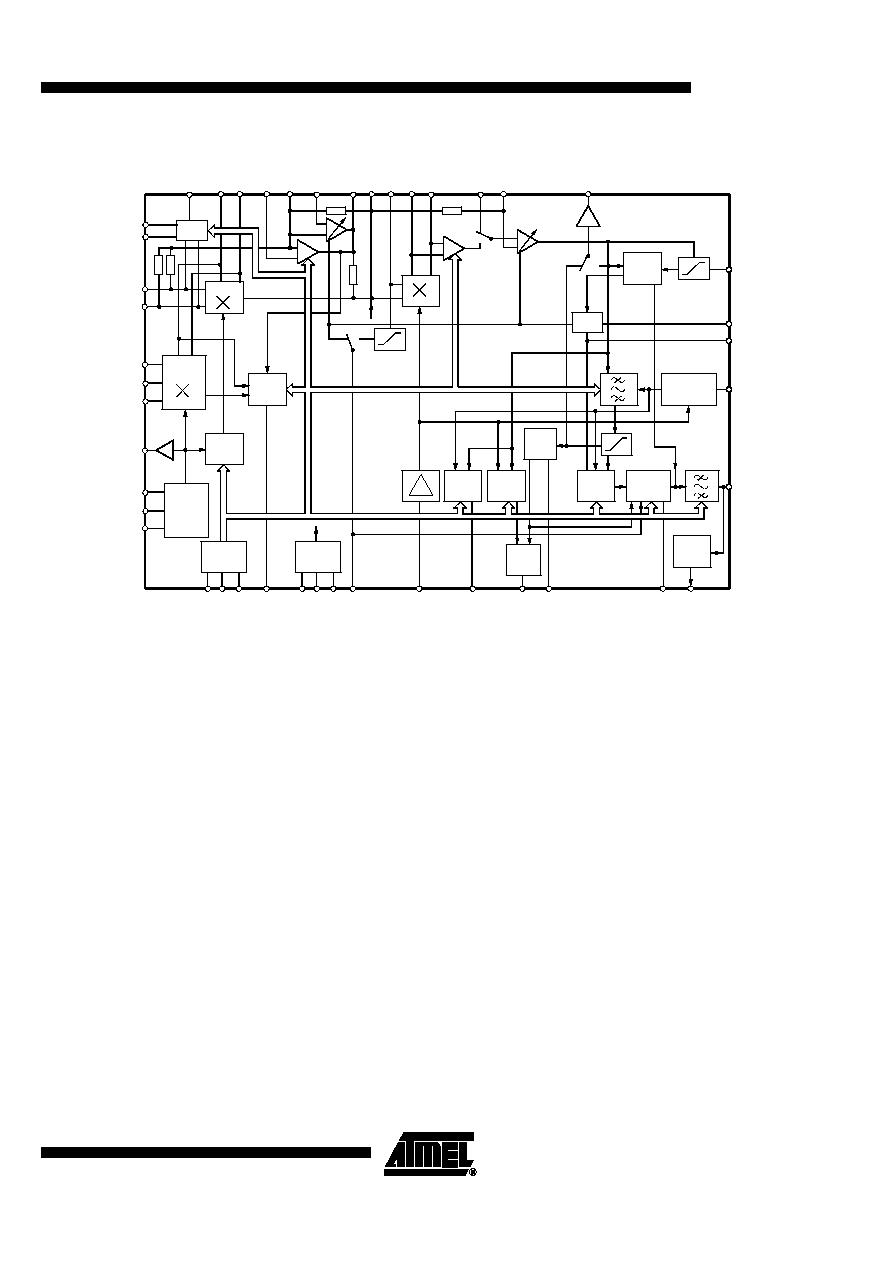
Figure 2. Block Diagram
Functional
Description
The U4255BM-M implements an AM up/down-conversion reception path from the RF
input signal to the AM-demodulated audio frequency output signal, and for FM reception
a double-conversion reception path from the RF input signal to the FM-demodulated
multiplex signal (MPX). A VCO and an LO prescaler for AM are integrated to generate
the LO frequency for the 1
st
mixer. Automatic gain control (AGC) circuits are imple-
mented to control the preamplifier and IF stages in the AM and FM reception path.
For improved FM performance, an integrated IF filter with adjustable bandwidth, a soft-
mute feature and an automatic multipath noise cancellation (MNC) circuit are fully
integrated. A powerful set of sensors is provided for receiving condition analysis and
stop signal generation.
Several register bits (Bit 0 to Bit 93) are used to control circuit operation and to adapt
certain circuit parameters to the specific application. The control bits are organized in
two 8-bit and three 24-bit registers that can be programmed by the 3-wire bus protocol.
The bus protocol and the bit-to-register mapping is described in the section '3-wire Bus
Description'. The meaning of the control bits is mentioned in the following sections.
Reception Mode
The IC can be operated in four different modes. Mode AM, FM, WB, Standby are
selected by means of Bit 92 and Bit 93 according to Table 1.
In AM mode the AM mixer, the AM RF-AGC and the 1
st
IF AM amplifier at Pin 33 are
activated. The input of the 2
nd
IF amplifier is connected to Pin 28 and the output of the
2
nd
IF amplifier is fed to the AM demodulator. The output of the AM demodulator is
available at MPX output Pin 11.
30 29
MX2IN
MX2OB
AM
4
3
2
7
6
41
26
23
AMAGC
AMVREG
MX1AMA
MX1AMB
GNDMX
MX1FMB
AMPLPF
MX1OA
IF1FMI
8
43
38
MX2OA
IF2IN
V3P
IF2OUT
24
28
27
20
IF1REF
IF1AMI
IF1OUT
V3
39
33
AGC
15
16
14
1
MX1FMA
OSCOUT
GNDOSC
OSCE
13
OSCB
MX1OB
44
FM
Divider
AM
FM
OSC
AGC
V3
Bus
FMAGC
EN
CLK
DATA
17 18 19
5
Bandgap
METER
V57
GND
VS
12 25 42 9
V3
ADJAC
MX2LO
22
10
DEV
INT
MULTIP
SMUTE
21
40
34
31
INT
Adj.
chan
.
Stop
Multi-
path
AGC
AM
dem.
32
36
35
37
11
OPLPF
IFAGCL
IFAGCCH
FILADJ
MPX
Automatic
adjustment
Soft
mute
Dev.
ana.
FM
dem.

4
U4255BM-M
4519C≠AUDR≠07/02
In FM mode the FM mixer, the FM RF-AGC and the 1
st
IF FM amplifier at Pin 38 are
activated. The bandwidth of the output tank at Pin 23, Pin 24 is increased and the input
of the 2
nd
IF amplifier can be switched between Pin 23, Pin 24 and Pin 28. The output of
the 2
nd
IF amplifier is fed to the integrated bandfilter and FM demodulator. The output of
the FM demodulator is available at MPX output Pin 11.
WB mode is similar to FM mode but the input of the 2
nd
IF amplifier is fixed to Pin 28, the
range of the bandwidth control of the integrated band filter is shifted to lower bandwidth
and the gain of the FM demodulator is increased.
In standby mode the mixers, IF amplifiers and AGC circuits are deactivated to reduce
current consumption.
Table 1. Operating Mode
Test Mode
A special test mode is implemented for final production test only. This mode is activated
by setting Bit 9 = 1.
This mode is not intended to be used in customer application.
For normal operation, Bit 9 has to be set to 0. Bit 18 to Bit 30 are deactivated in normal
operation mode.
Table 2. Test Mode
VCO
An oscillator circuit is implemented to build a VCO as proposed in the application sche-
matic. The VCO frequency is used to generate the LO frequency of the 1
st
mixer stages.
The control voltage of the VCO is usually generated by the PLL circuit U4256BM. The
VCO signal is provided at the buffered output Pin 16 to be fed to the PLL circuit.
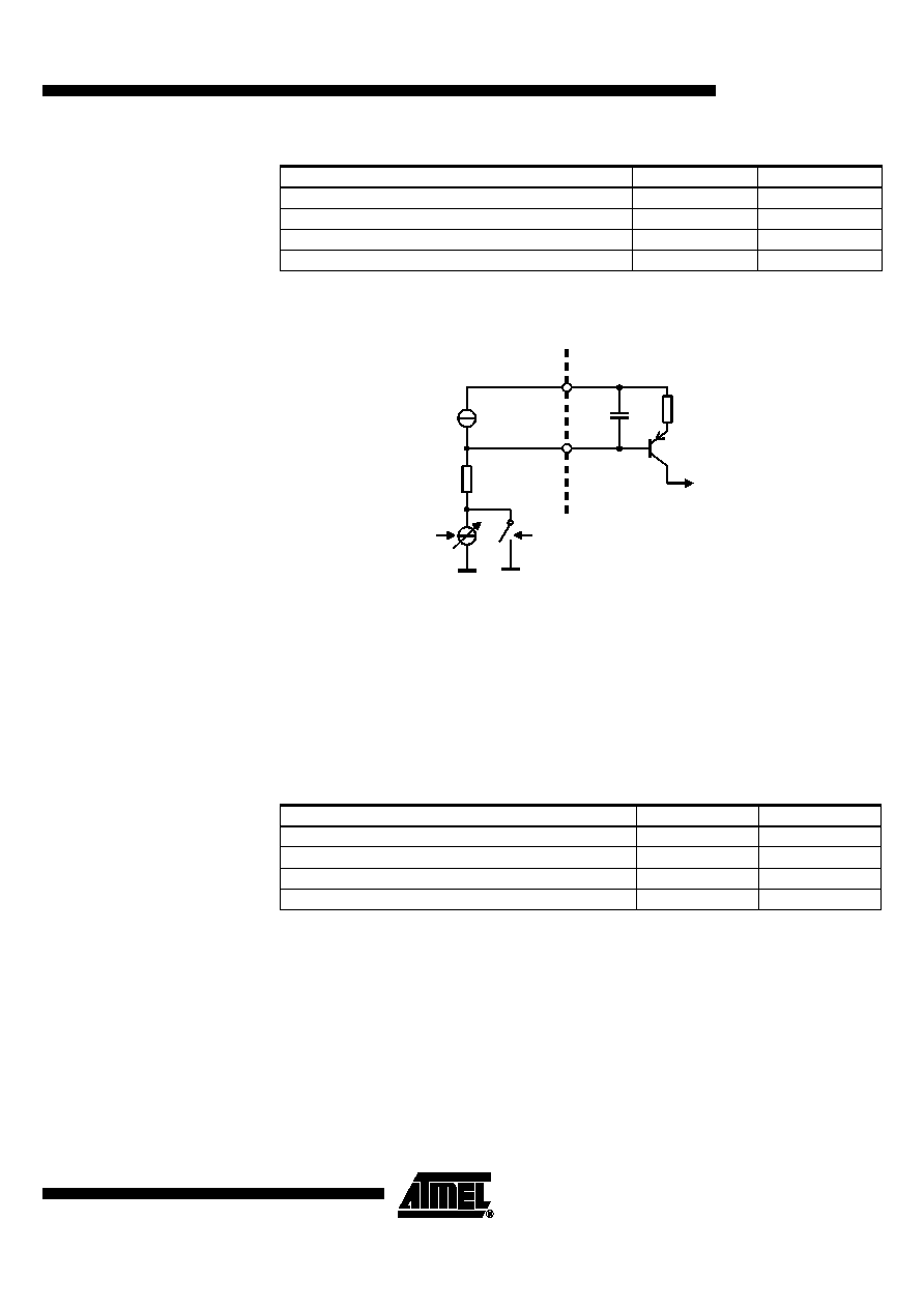
FM RF-AGC
The FM RF-AGC circuit includes a wideband level detector at the input Pin 1 of the FM
mixer and an in-band level detector at the output of the FM IF amplifier (Pin 30). The
outputs of these level detectors are used to control the current into the pin diode (see
Figure 3) in order to limit the signal level at the FM mixer input and the following stages.
The maximum pin diode current is determined by R115 and the time constant of the
AGC control loop can be adjusted by changing the value of C111.
The AGC threshold level at the input of the FM mixer can be adjusted by Bit 64 and
Bit 65 according to Table 3. The in-band AGC threshold referred to the FM mixer input
(Pin 1, Pin 2) depends on the gain of the FM IF amplifier and can be adjusted by Bit 89
to Bit 91.
AM/FM/Weather Channel
Bit 93
Bit 92
Standby
0
0
FM
0
1
AM
1
0
Weather band
1
1
Mode
Bit 9
Normal operation
0
Testmode
1
5
U4255BM-M
4519C≠AUDR≠07/02
Table 3. FM-AGC Threshold
Figure 3. FM RF-AGC Bit 92
AM RF-AGC
The AM RF-AGC controls the current into the AM pin diodes (Pin 7) and the source
drain voltage of the MOSFET in the AM preamplifier stage (Pin 6) to limit the level at the
AM mixer input (Pin 3, Pin 41). This threshold level can be set by Bit 62 and Bit 63. If the
level at the AM mixer input exceeds the selected threshold, the current into the AM pin
diodes is increased. If this step is not sufficient, the source drain voltage of the MOSFET
is decreased. The time constant of the AGC control loop can be adjusted by changing
the value of the capacitor at Pin 8.
Table 4. AM-AGC Threshold
FM 1
st
Mixer
In the 1
st
FM mixer stage, the FM reception frequency is down converted to the 1
st
IF
frequency. The VCO frequency is used as LO frequency for the mixer.
AM 1
st
Mixer
The AM 1
st
mixer is used for up-conversion of the AM reception frequency to the 1
st
IF
frequency. Therefore, an AM prescaler is implemented to generate the necessary LO
frequency from the VCO frequency. The divide factor of the AM prescaler can be
selected according to Table 5.
FM-AGC Threshold
Bit 65
Bit 64
104 dB
m
V
0
0
101 dB
m
V
0
1
98 dB
m
V
1
0
92 dB
m
V
1
1
AGC
B92
PIN Diode
VS Pin 42
Pin 5
C111
R115
AM-AGC Threshold
Bit 63
Bit 62
99 dB
m
V
0
0
102 dB
m
V
0
1
104 dB
m
V
1
0
105 dB
m
V
1
1