 | –≠–ª–µ–∫—Ç—Ä–æ–Ω–Ω—ã–π –∫–æ–º–ø–æ–Ω–µ–Ω—Ç: U4311B-M | –°–∫–∞—á–∞—Ç—å:  PDF PDF  ZIP ZIP |
U4311B
Rev. A3, 28-Sep-00
1 (15)
Low-Current Superhet Remote Control Receiver
Description
The U4311B is a monolithic integrated circuit in bipolar
technology for low-current UHF remote control super-
heterodyne receivers in amplitude- or frequency-
modulated mode. Typical applications are keyless car
lock-, alarm- or tele-control remote indication systems.
Especially for automotive applications, it supports a
superhet design with about 1 mA total current
consumption as required by the car manufacturers.
Features
D Usable for amplitude- and frequency-modulated
transmission systems
D Extremely low quiescent current (approximately
1 mA in standby mode due to wake-up concept)
D Wide power supply voltage range 3 to 13 V
D Sensitive IF amplifier for 10.7-MHz operating
frequency
D Logarithmic AM demodulator
D FM demodulator
D Monoflop exit to wake up a microcontroller
D High-performance operational amplifier to realize a
data recovering filter
D Non-inverting clamping comparator with amplitude-
depending hysteresis for data regeneration
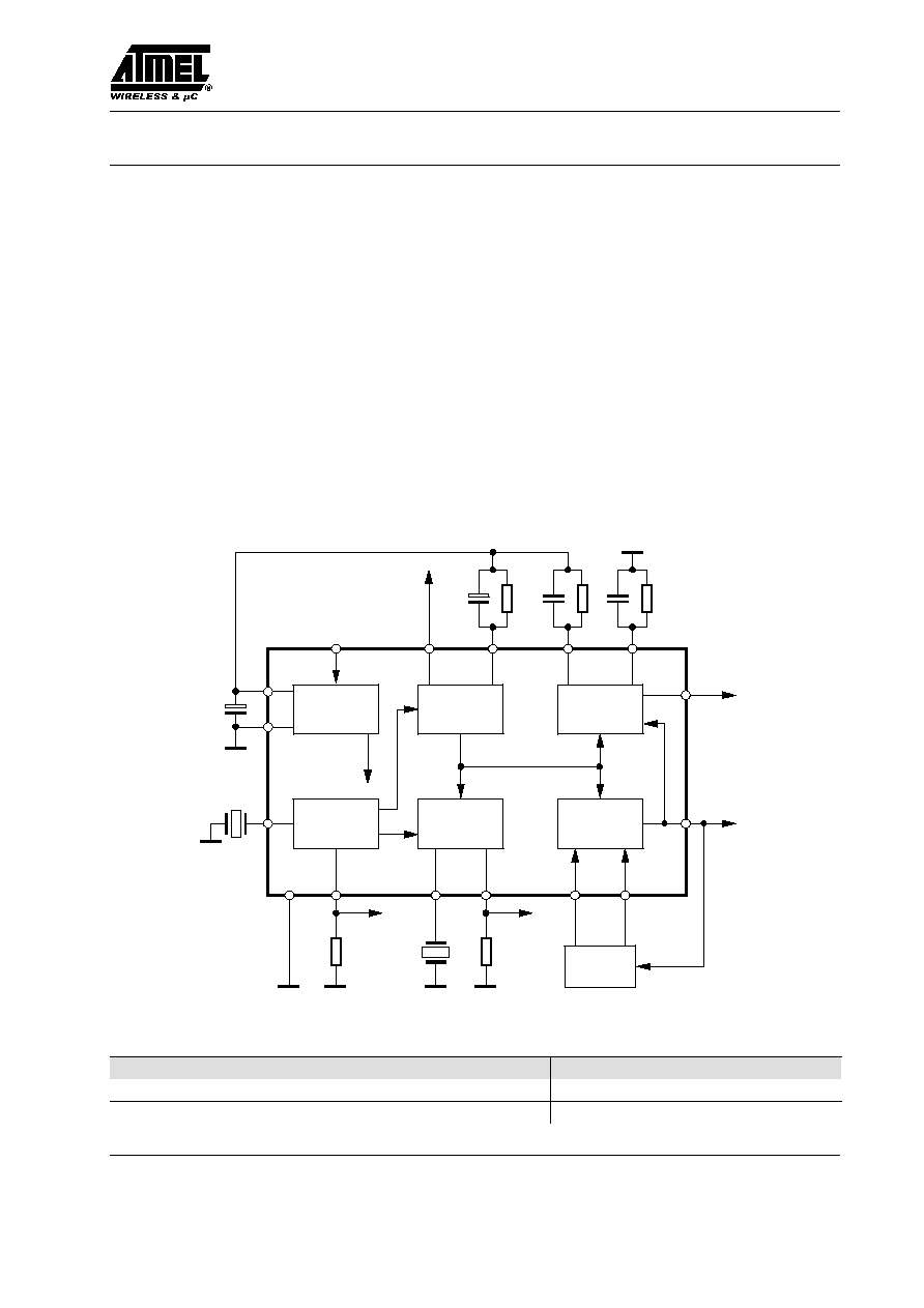
Block Diagram
Non ≠ invert.
clamping
comparator
Monoflop
Bandgap
Quadrature
detector
Operational
amplifier
IF
amplifier
Internal
RF
Level
Wake up
10
3
Wake-up out
7
6
V
S
2
5
+
≠
16
1
14
12
8
Data out
Data
filter
FM out
log AM out
10.7 MHz
10.7 MHz
13
11
V
Ref
= 2.4V
4
95 9968
V
Ref
= 2.4 V
9
15
Figure 1. Block diagram
Ordering Information
Extended Type Number
Package
Remarks
U4311B-M
DIP16
U4311B-MFL
SO16L

U4311B
Rev. A3, 28-Sep-00
2 (15)
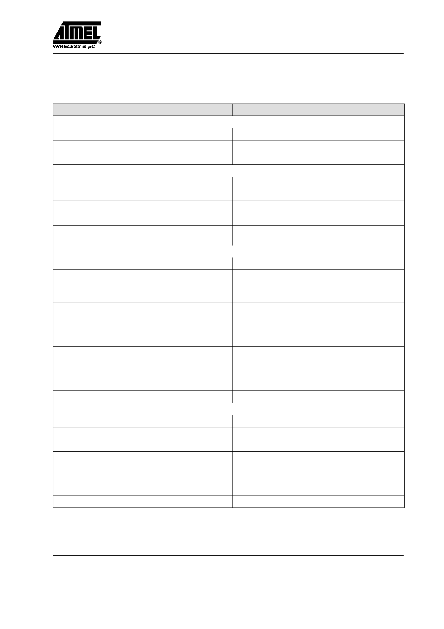
Pin Description
1
2
3
4
5
6
7
8
16
15
14
13
12
11
10
9
RC
wake
GND2
95 10322
Comp
out
RC≠
RC+
AM
out
OP
in+
OP
out
FM
out
V
Ref
Discr
GND1
SW
out
IF
in
OP
in≠
V
S
Figure 2. Pin description
Pin
Symbol
Function
1
OP
in+
OP amplifier non-inverted input
2
OP
out
OP amplifier output
3
RC
wake
RC wake-up reset time
4
GND2
Ground of the logical circuits
5
Comp
out
Comparator output
6
RC≠
Comparator time constant
7
RC+
Comparator time constant
8
AM
out
AM current output
9
IF
in
IF input
10
SW
out
Wake-up output
11
GND1
Ground of the analog circuits
12
Discr
FM discriminator tank
13
V
Ref
Reference voltage
14
FM
out
FM discriminator output
15
V
S
Supply voltage
16
OP
in≠
OP amplifier inverted input
Internal connections see figures 4 to 19
Absolute Maximum Ratings
Parameters
Symbol
Value
Unit
Supply voltage
V
S
13
V
Power dissipation
T
amb
= 85
∞C
P
tot
400
mW
Junction temperature
T
j
125
∞C
Ambient temperature
T
amb
≠40 to +85
∞C
Storage temperature
T
stg
≠55 to +125
∞C
Thermal Resistance
Parameters
Symbol
Value
Unit
Junction ambient
DIP16
SO16L
R
thJA
R
thJA
120
100
K/W
K/W
U4311B
Rev. A3, 28-Sep-00
3 (15)
Electrical Characteristics
V
S
= 5 V, T
amb
= 25
∞C, f
in
= 10.7 MHz; FM part: f
mod
= 1 kHz, f
dev
= 22.5 kHz; AM part: f
mod
= 1 kHz, m = 100%
unless otherwise specified
Parameters
Test Conditions / Pins
Symbol
Min.
Typ.
Max.
Unit
Characteristics
Supply-voltage range
Pin 15
V
S
3
12
V
Quiescent supply current
Pin 15
I
q
1
1.3
mA
Active supply current
Pin 15
I
act
2.8
3.6
mA
Bandgap
Regulated voltage
Pin 13
V
Ref
2.3
2.4
2.5
V
Output current
Pin 13
I
Ref
5
mA
Source resistance
Pin 13
R
Ref
2.3
5
W
External capacitor
Pin 13
C
Ref
10
mF
Power-supply rejection
ratio
f = 50 Hz
Pin 13
psrr
60
dB
IF amplifier
Input resistance
Pin 9
R
in
180
330
520
W
Input capacitance
Pin 9
C
in
5
pF
Typical internal 3 dB
frequency
IF level 70 dB
mV
Pins 9 and 14
f
3dB
8
12
MHz
≠3 dB limiting point
Pin 9
V
FM3dB
30
dB
mV
Recovered data voltage
Pin 14
V
FMout
50
130
230
mV
FM detector output
resistance
Pin 14
R
FMout
50
k
W
AM rejection ratio
m = 30%
Pins 9 and 14
AM
rr
25
dB
Maximum AM input
voltage
Pin 9
V
AMmax
90
dB
mV
AM quiescent current
Pin 8
I
AMout
10
22
37
mA
Maximum AM current
Pin 8
I
AMoutmax
100
mA
Operational amplifier
Gain-bandwidth product
Pins 1, 2 and 16
f
t
3
4
6.5
MHz
Excess phase
Pins 1, 2 and 16
d
80
degree
Open loop gain
Pins 1, 2 and 16
g
0
50
70
95
dB
Output voltage range
Pin 2
V
out
1.55
V
Common-mode input
voltage
Pins 1 and 16
V
in
0.7
1.7
V
Input offset voltage
Pins 1 and 16
V
os
≠2.5
0
+2.5
mV
Maximum output current
Pin 2
I
out
5
mA

U4311B
Rev. A3, 28-Sep-00
4 (15)
Unit
Max.
Typ.
Min.
Symbol
Test Conditions / Pins
Parameters
Common-mode rejection
ratio
Pin 1 and 16
cmrr
65
85
dB
Total harmonic distortion
V
in
< 300 mV, f = 33 kHz,
unity gain circuit Pin 2
thd
1
3
%
U4311B
Rev. A3, 28-Sep-00
5 (15)
Electrical Characteristics (continued)
V
S
= 5 V, T
amb
= 25
∞C, f
in
= 10.7 MHz; FM part: f
mod
= 1 kHz, f
dev
= 22.5 kHz; AM part: f
mod
= 1 kHz, m = 100%
unless otherwise specified
Parameters
Test Conditions / Pins
Symbol
Min.
Typ.
Max.
Unit
Power-supply rejection
ratio
f = 50 Hz
Pin 2
psrr
65
85
dB
Clamping comparator
Typical common-mode
input voltage range
Pin 2
V
cmvr
0.8
1.6
V
Maximum distortion
voltage
V
signal
= 100 mV,
R+ = R≠ = 50 k
W,
C+ = C≠ = 200 nF,
f
disto
= 50 Hz,
f
signal
= 1 kHz
Pin 2
V
dmax
200
mV
Output voltage
V
2
> (V
6
+ V
7
) /2
(10-k
W load to V
Ref
)
Pin 5
V
cout
V
Ref
V
Output voltage
V
2
< (V
6
+ V
7
) /2
(10-k
W load to V
Ref
)
Pin 5
V
cout
0
150
250
mV
Wake-up circuit
Minimum wake-up level
Pin 9
V
in
40
dB
mV
1)
Internal charging resistor
Pin 3
R
int
1.5
k
W
Threshold voltage
Pin 3
V
th
1.6
V
Output switch current
Pin 10
I
SW
180
250
550
mA
Output switch voltage
Pin 10
V
SW
5.5
V
2)
External wake-up resistor
Pins 3 and 13
R
WU
22
k
W
External wake-up capacitor
Pins 3 and 13
C
WU
10
mF
Hold time (
± 30%)
t
h
1.5 R
WU
C
WU
s
3)
Delay time (
± 30%)
t
d
C
WU
0.75 kW
s
3)
1)
Measured at Pin 9, referred to 330
W
2)
Protected by a Z-diode, see figure 13
3)
Valid for 0.1
mF C
WU
10 mF and 22 kW R
WU
680 kW