U4311B-FS
Rev. A3, 28-Sep-00
1 (13)
Low-Current Superhet Remote Control Receiver
Description
The U4311B-FS is a monolithic integrated circuit in
bipolar technology for low-current UHF remote control
super-heterodyne receivers in amplitude- or frequency-
modulated mode. Typical applications are keyless car
lock-, alarm- or tele-control remote indication systems.
Especially for automotive applications, it supports a
superhet design with about 1 mA total current
consumption as required by the car manufacturers.
Features
D Usable for amplitude- and frequency-modulated
transmission systems
D Extremely low quiescent current (approximately
1 mA in standby mode due to wake-up concept)
D Wide power supply voltage range 3 to 13 V
D Sensitive IF amplifier for 10.7-MHz operating
frequency
D Logarithmic AM demodulator
D FM demodulator
D Monoflop output to wake up a microcontroller
D High-performance operational amplifier to realize a
data recovering filter
D Non-inverting clamping comparator with amplitude-
depending hysteresis for data regeneration
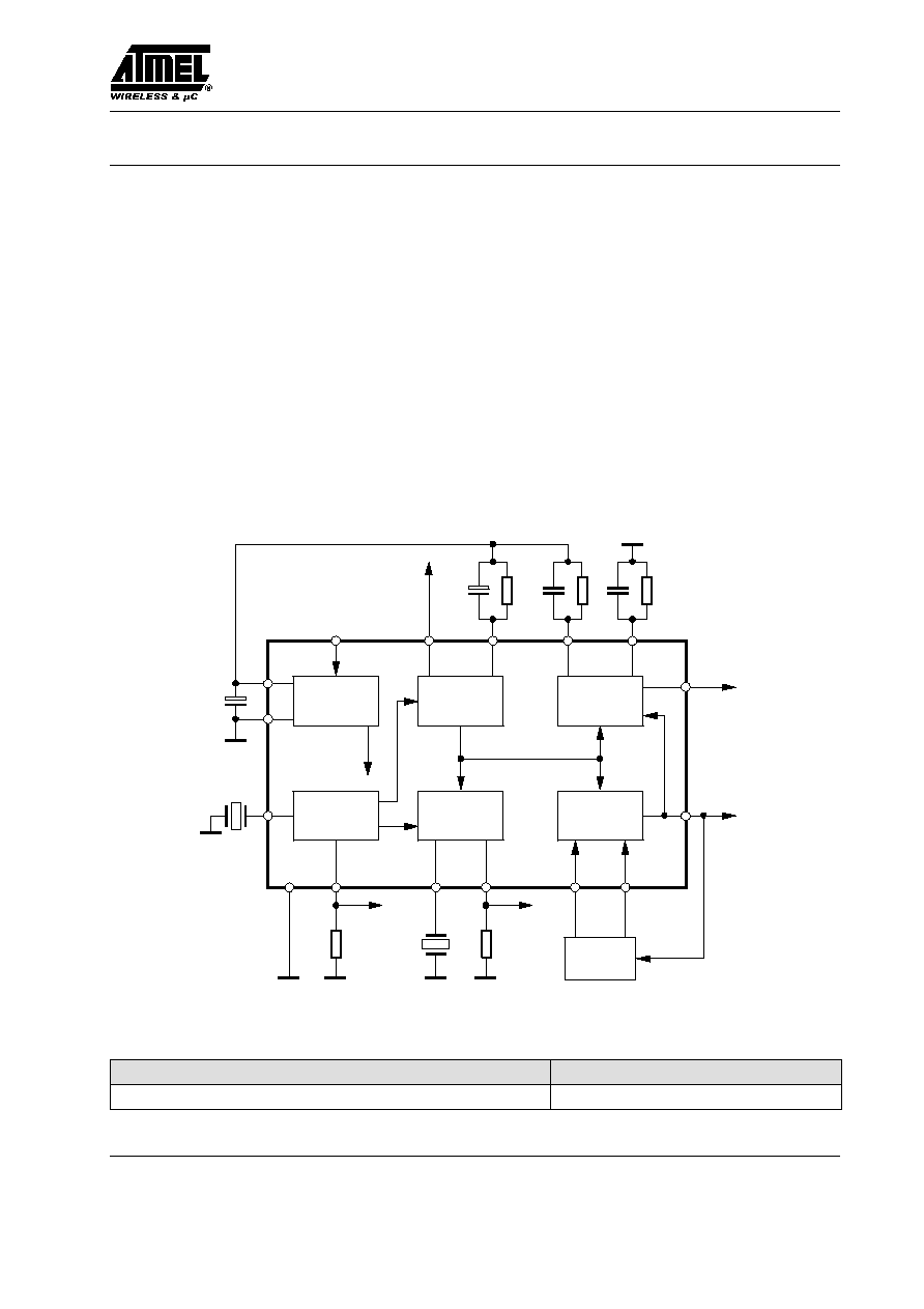
Block Diagram
Non ≠ invert.
clamping
comparator
Monoflop
Bandgap
Quadrature
detector
Operational
amplifier
IF
amplifier
Internal
RF
Level
Wake up
13
3
Wake-up out
9
7
V
S
2
6
+
≠
20
1
18
16
11
Data out
Data
filter
FM out
log AM out
10.7 MHz
10.7 MHz
17
15
V
Ref
= 2.4V
5
12648
V
Ref
= 2.4 V
12
19
Figure 1. Block diagram
Ordering Information
Extended Type Number
Package
Remarks
U4311B-MFSG3
SSO20
Ambient temperature up to +105
∞
C
U4311B-FS
Rev. A3, 28-Sep-00
2 (13)
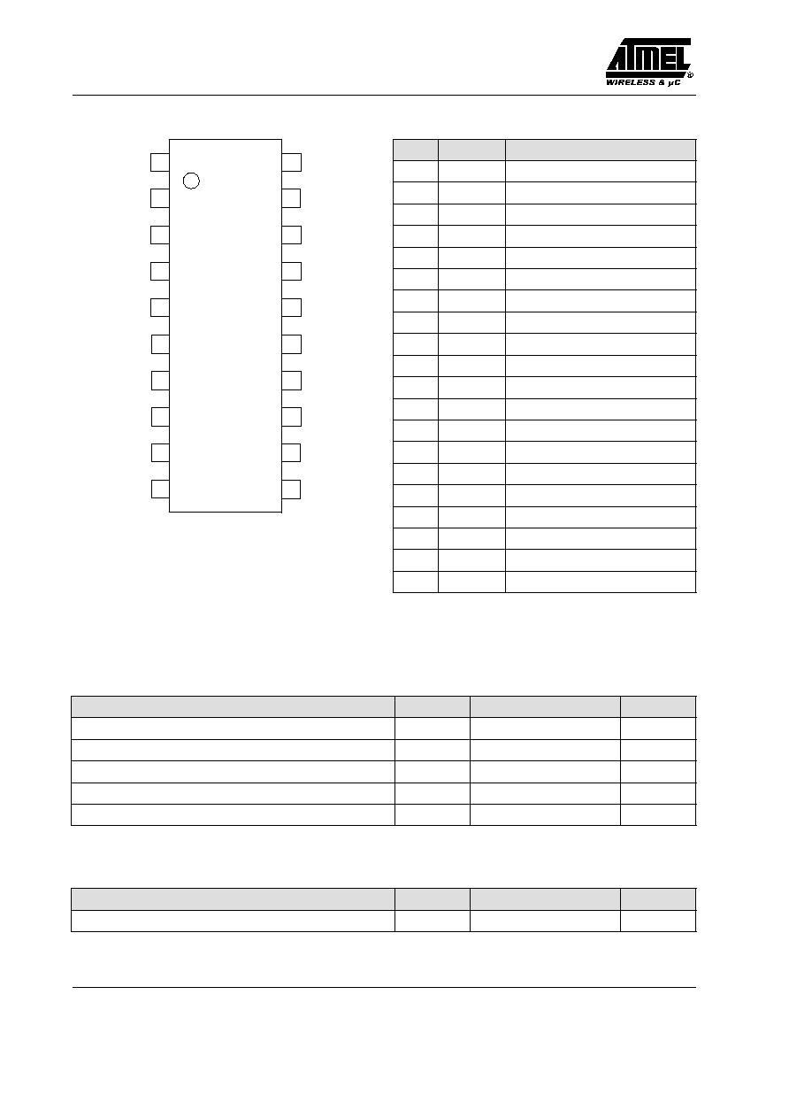
Pin Description
1
2
3
4
5
6
7
8
10
9
19
18
17
16
14
15
13
12
11
20
n.c.
GND2
12649
Comp
out
RC≠
n.c.
RC+
OP
out
RC
wake
V
Ref
Discr
GND1
n.c.
SW
out
IF
in
V
S
FM
out
n.c.
AM
out
OP
in+
OP
in≠
Figure 2. Pinning
Pin
Symbol
Function
1
OP
in+
OP amplifier non-inverted input
2
OP
out
OP amplifier output
3
RC
wake
RC wake≠up reset time
4
n.c.
Not connected
5
GND2
Ground of the logical circuits
6
Comp
out
Comparator output
7
RC≠
Comparator time constant
8
n.c.
Not connected
9
RC+
Comparator time constant
10
n.c.
Not connected
11
AM
out
AM current output
12
IF
in
IF input
13
SW
out
Wake-up output
14
n.c.
Not connected
15
GND1
Ground of the analog circuits
16
Discr
FM discriminator tank
17
V
Ref
Reference voltage
18
FM
out
FM discriminator output
19
V
S
Supply voltage
20
OP
in≠
OP amplifier inverted input
Internal connections see figures 4 to 19
Absolute Maximum Ratings
Parameters
Symbol
Value
Unit
Supply voltage
V
S
13
V
Power dissipation
T
amb
= 85
∞
C
P
tot
400
mW
Junction temperature
T
j
125
∞
C
Storage temperature
T
stg
≠55 to +125
∞
C
Ambient temperature for SSO20
T
amb
≠40 to +105
∞
C
Thermal Resistance
Parameters
Symbol
Value
Unit
Junction ambient
SSO20
R
thJA
140
K/W

U4311B-FS
Rev. A3, 28-Sep-00
3 (13)
Electrical Characteristics
V
S
= 5 V, T
amb
= 25
∞
C, f
in
= 10.7 MHz; FM part: f
mod
= 1 kHz, f
dev
= 22.5 kHz; AM part: f
mod
= 1 kHz, m = 100%
unless otherwise specified
Parameters
Test Conditions / Pins
Symbol
Min.
Typ.
Max.
Unit
Characteristics
Supply-voltage range
Pin 19
V
S
3
12
V
Quiescent supply current
Pin 19
I
q
1
1.3
mA
Active supply current
Pin 19
I
act
2.8
3.6
mA
Bandgap
Regulated voltage
Pin 17
V
Ref
2.3
2.4
2.5
V
Output current
Pin 17
I
Ref
5
mA
Source resistance
Pin 17
R
Ref
2.3
5
W
External capacitor
Pin 17
C
Ref
10
mF
Power-supply rejection
ratio
f = 50 Hz
Pin 17
psrr
60
dB
IF amplifier
Input resistance
Pin 12
R
in
180
330
520
W
Input capacitance
Pin 12
C
in
5
pF
Typical internal 3 dB
frequency
IF level 70 dB
mV
Pins 12 and 18
f
3dB
8
12
MHz
≠3 dB limiting point
Pin 12
V
FM3dB
30
dB
mV
Recovered data voltage
Pin 18
V
FMout
50
130
230
mV
FM detector output
resistance
Pin 18
R
FMout
50
k
W
AM rejection ratio
m = 30% Pins 12 and 18
AM
rr
25
dB
Maximum AM input
voltage
Pin 12
V
AMmax
90
dB
mV
AM quiescent current
Pin 11
I
AMout
10
22
37
mA
Maximum AM current
Pin 11
I
AMoutmax
100
mA
Operational amplifier
Gain-bandwidth product
Pins 1, 2 and 20
f
t
3
4
6.5
MHz
Excess phase
Pins 1, 2 and 20
d
80
degree
Open loop gain
Pins 1, 2 and 20
g
0
50
70
95
dB
Output voltage range
Pin 2
V
out
1.55
V
Common mode input
voltage
Pins 1 and 20
V
in
0.7
1.7
V
Input offset voltage
Pins 1 and 20
V
os
≠2.5
0
+2.5
mV
Maximum output current
Pin 2
I
out
5
mA
Common-mode rejection
ratio
Pin 1 and 20
cmrr
65
85
dB
Total harmonic distortion
V
in
< 300 mV, f = 33 kHz,
unity gain circuit Pin 2
thd
1
3
%

U4311B-FS
Rev. A3, 28-Sep-00
4 (13)
Electrical Characteristics (continued)
V
S
= 5 V, T
amb
= 25
∞
C, f
in
= 10.7 MHz; FM part: f
mod
= 1 kHz, f
dev
= 22.5 kHz; AM part: f
mod
= 1 kHz, m = 100%
unless otherwise specified
Parameters
Test Conditions / Pins
Symbol
Min.
Typ.
Max.
Unit
Power-supply rejection
ratio
f = 50 Hz
Pin 2
psrr
65
85
dB
Clamping comparator
Typical common-mode
input voltage range
Pin 2
V
cmvr
0.8
1.6
V
Maximum distortion
voltage
V
signal
= 100 mV,
R+ = R≠ = 50 k
W,
C+ = C≠ = 200 nF,
f
disto
= 50 Hz,
f
signal
= 1 kHz Pin 2
V
dmax
200
mV
Output voltage
V
2
> (V
7
+ V
9
) /2
(10-k
W load to V
Ref
)
Pin 6
V
cout
V
Ref
V
Output voltage
V
2
< (V
7
+ V
9
) /2
(10-k
W load to V
Ref
)
Pin 6
V
cout
0
150
250
mV
Wake-up circuit
Minimum wake-up level
Pin 12
V
in
40
dB
mV
1)
Internal charging resistor
Pin 3
R
int
1.5
k
W
Threshold voltage
Pin 3
V
th
1.6
V
Output switch current
Pin 13
I
SW
180
250
550
mA
Output switch voltage
Pin 13
V
SW
5.5
V
2)
External wake-up resistor
Pins 3 and 17
R
WU
22
k
W
External wake-up capacitor
Pins 3 and 17
C
WU
10
mF
Hold time (
±
30%)
t
h
1.5 R
WU
C
WU
s
3)
Delay time (
±
30%)
t
d
C
WU
0.75 kW
s
3)
1)
Measured at Pin 9, (12) referred to 330
W
2)
Protected by a Z-diode, see figure 13
3)
Valid for 0.1
mF
C
WU
10
mF and 22 kW
R
WU
680 k
W
U4311B-FS
Rev. A3, 28-Sep-00
5 (13)
Circuit Description
General Functions
The integrated circuit U4311B-FS includes the following
functions: IF amplifier, FM demodulator, wake-up circuit
with monoflop, operational amplifier, non-inverting data
comparator and voltage regulator.
The 10.7-MHz IF signal from the front end passes the
integrated IF amplifier which operates for amplitude- or
frequency-modulated signals to either a logarithmic AM
demodulator which was implemented to avoid settling-
time problems effected by use of an automatic gain
control system or a quadrature detector for FM. A data-
shaping filter
* advantageously realized with the
internal high-performance operational amplifier
*
reduces system bandwidth to an optimized compromise
regarding transmission distance and data recognition.
Thus, an optimal bit-error rate can be achieved without
any further active component.
The comparator connected to the output of the filter has
a level-dependent hysteresis and clamps its reference
voltage to the signal's minimum and maximum peaks as
described later.
Without IF-input signal
* in normal mode * only the IF
amplifier and the AM demodulator which operates as a
level-strength indicator are activated. If the level of the IF
signal increases, the entire circuitry is turned on by the
wake-up circuit. This signal is externally available at
Pin 13 and can be used to wake up a microcontroller.
After an adjustable reset time, determined by the mono-
flop time constant, the integrated circuit returns to sleep
mode. In this case, typically 1-mA supply current is re-
quired. An external resistor matched at Pin 3 to ground
blocks the wake-up circuit and enables the complete func-
tionally at lower IF level as can be seen in figures 24
and 27, but supply current increases up to typically
2.8 mA.
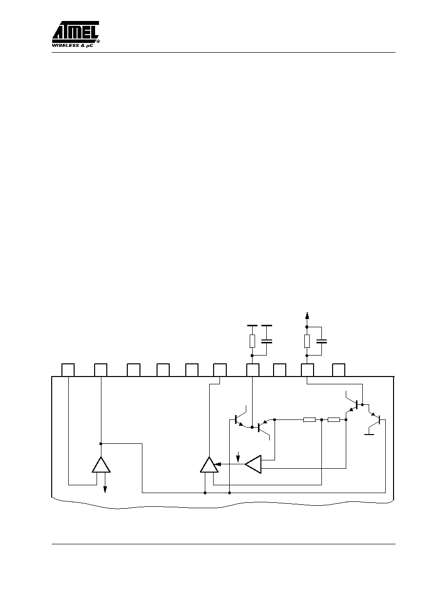
Function of the Clamping Comparator
The output signal of the operational amplifier is fed to the
input of the non-inverting comparator and two peak
detectors (Q1 and Q2, figure 3). Their time constants are
distinguished by RC+ and RC≠. The component's value
must be adapted to the transmission code. The time
constant should be large compared to the bit rate for opti-
mized noise and hum suppression. To compensate the
input transistor's base-emitter-voltage differences, these
two signals are buffered by Q3 and Q4. The mean value
is used as comparator threshold, the difference of the peak
values controls the hysteresis. This clamping comparator
operates as a data regenerator.
1
2
3
4
5
6
7
8
Hysteresis
Comp. threshold
Comparator
Op. amp.
+ ≠
Q1
Q3
Q4
Q2
V
Ref
to Pin 20
12650
10
9
Figure 3. Principle function of the clamping comparator