Rev. 4775A≠AUTO≠11/03
Features
∑
2-kV ESD Protection
∑
Two Comparators with Common Reference
∑
Tight Threshold Tolerance
∑
Threshold Matched to PTC Characteristic of Incandescent Lamps
∑
Temperature Compensated
∑
NPN Output
∑
Interference and Damage-protection According to VDE 0839
∑
EMI Protection
∑
Reversal Polarity Protection
∑
Load-dump Protection
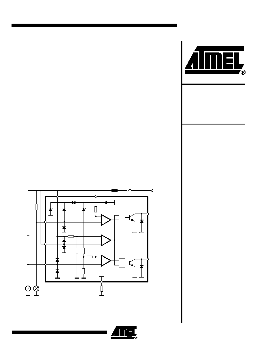
Description
The monolithic integrated bipolar circuit, U479B, is designed as a monitor for lamp fail-
ure in automobiles. The comparator threshold is matched to the PTC characteristic of
incandescent lamps. The threshold is tied to V
4,6
= V
S
- V
T
where V
T
= 8 mV.
If the voltage drop across the shunt resistor, R
sh
, exceeds 8 mV, the output is turned
off, otherwise, the output is turned on. Without supply voltage or open input pin 8, the
output is turned off. A comparator input, which is not used, must be connected to
pin 7.
Figure 1. Schematic and Application Circuit
-
+
-
+
-
+
&
&
2
7
4
8
6
5
3
1
150
V
S
Lamps
0.6 V
S
OUT1
OUT2
V
Batt
Z
2
R
sh
R
sh
R
1
Automotive
Lamp-outage
Monitor IC
U479B
3
U479B
4775A≠AUTO≠11/03
Absolute Maximum Ratings
Stresses beyond those listed under "Absolute Maximum Ratings" may cause permanent damage to the device. This is a stress rating
only and functional operation of the device at these or any other conditions beyond those indicated in the operational sections of this
specification is not implied. Exposure to absolute maximum rating conditions for extended periods may affect device reliability.
Parameters
Pin
Symbol
Value
Unit
Supply voltage
2, 7
V
S
16.5
V
Current consumption, t = 2 ms
1
I
1
1.5
A
Output current
3, 5
I
3,5
20
mA
Input voltage
Reference point pin 7
4, 6
-V
4,6
6
V
Power dissipation
T
amb
= 95
∞
C
DIP8
SO8
P
tot
P
tot
420
360
mW
mW
T
amb
= 60
∞
C
DIP8
SO8
P
tot
P
tot
690
560
mW
mW
Ambient temperature range
T
amb
-40 to +95
∞
C
Storage temperature range
T
stg
-55 to +125
∞
C
Junction temperature
T
j
150
∞
C
Thermal Resistance
Parameters
Symbol
Value
Unit
Junction ambient
DIP8
R
thJA
110
K/W
SO8
R
thJA
160
K/W
4
U479B
4775A≠AUTO≠11/03
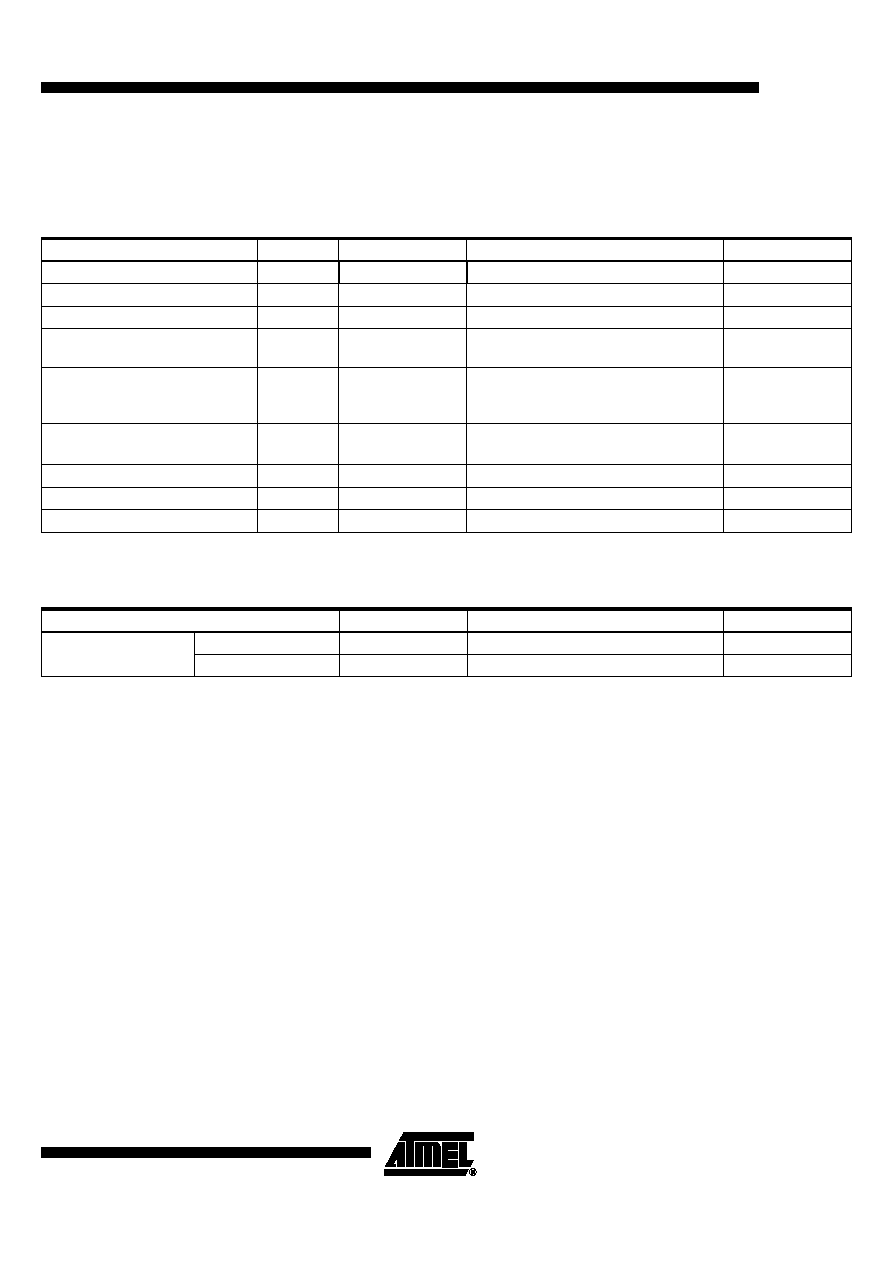
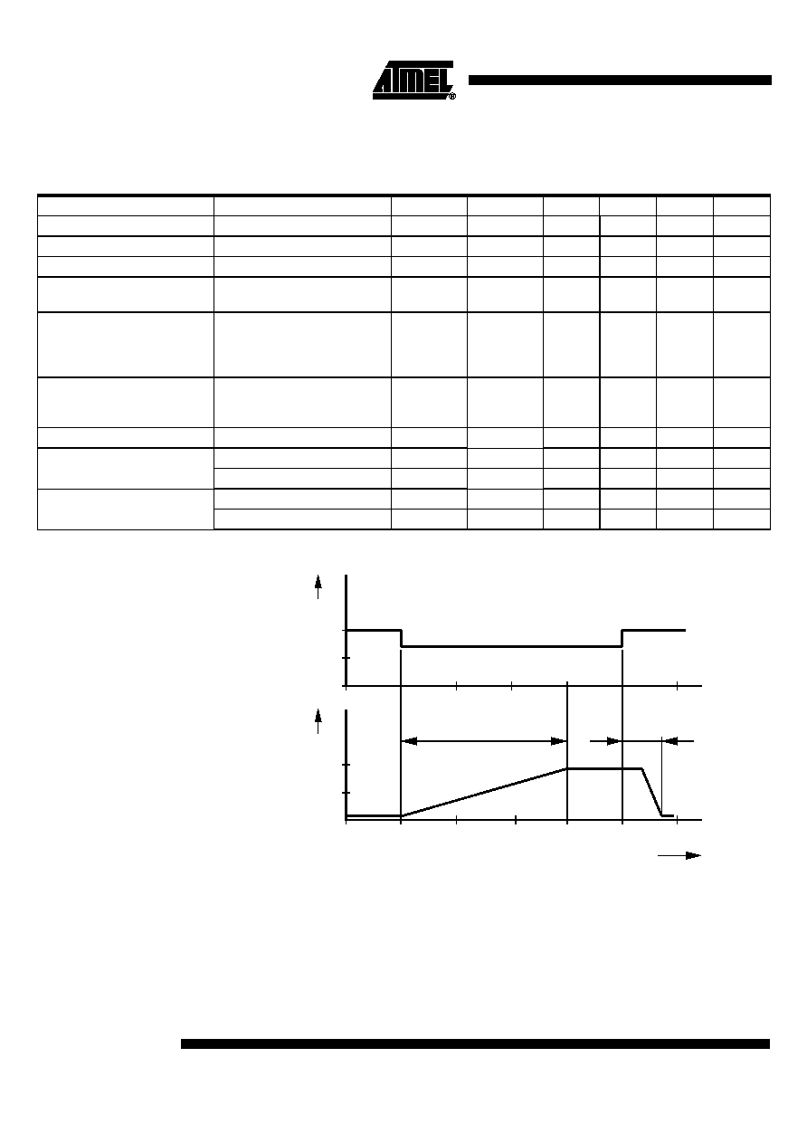
Figure 3. Delay Times
Electrical Characteristics
V
S
= 9 to 15 V, T
amb
= -40 to +95
∞
C, Figure 1 on page 1, unless otherwise specified.
Parameters
Test Conditions
Pin
Symbol
Min.
Typ.
Max.
Unit
Supply voltage
2, 7
V
S
9
15
V
Internal Z-diode Z
2
2
V
Z
20
V
Current consumption
V
S
= 12 V
1
I
1
4.5
6
mA
Output saturation voltage
V
S
= 9 V, I
3,5
= 10 mA
T
amb
= 25
∞
C
3, 5
V
sat
0.5
V
Control signal threshold
Reference point V
Pin 7
I
3,5
= 3 mA
V
S
= 12 V
V
S
= 15 V
4, 6
-V
T
-V
T
6.5
7.8
8
9.3
9.5
10.8
mV
mV
Voltage drift
D
V
0.45
mV/V
Threshold voltage
Switch identification
8
V
8
0.6 V
S
V
Input currents
Input 1/input 2
4, 6
I
I
100
nA
Input switch
8
I
I
5
µA
Delay time
Switch-on, high to low
3, 5
t
d(on)
6
µs
Switch-off, low to high
t
d(off)
30
µs
D
V
V
T(15 V)
V
T(12 V)
≠
15 V
12 V
≠
---------------------------------------------
=
12.00
11.95
12
V
0
t
d(on)
10
20
30
40
50
60 µs
0
t
V
V
6
t
d(off)
V
4,6