U490B
Rev. A3, 12-Jan-01
1 (6)
One-Shot Phase-Control IC
Description
The monolithic integrated bipolar circuit, U490B, is a
one-shot power control circuit, designed to control the
thyristor which is mainly used in electric stapler devices.
The IC is preferred to realise a one-shot phase control,
where any phase angle and thus any intensity of the load
voltage is adjustable. After successful triggering and the
following delay time, an ignition pulse at the output is re-
leased. A further triggering is only possible after the
elapse of the delay time.
Features
D Phase controlled thyristor ignition
D Triggering with time delay
D Repetition time delay
D Supply current
x
2 mA
D Mains supply via resistor
Applications
D Electric stapler devices
Block Diagram
Trigger
control
Repetition
delay
Start
delay
Sync.
Supply
stage
3
8
4
Phase control
Control
input
Ramp
POR
Output
stage
6
5
2
C
5
R
5
C
6
R
4
R
7
C
4
C
7
D
2
Load
C
2
R
2
V
S
R
1
D
1
R
3
C
3
S
1
L
N
220 k
W
1.5 nF
24 k
W/
2 W
1N4007
47
mF
10 V
230 V
X
V
mains
GND
150 nF
47 k
W
[68 kW
220 k
W
47 nF
7
150 nF
33
W
220
W
47 nF/
250 V
X
22 nF
C
1
U490B
Figure 1. Block diagram with external circuit
Ordering Information
Extended Type Number
Package
Remarks
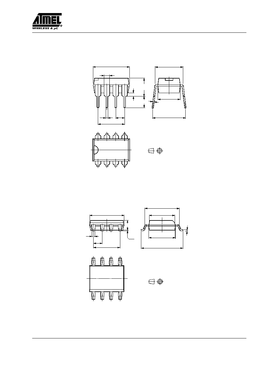
U490B-x
DIP8
Tube
U490B-xFP
SO8
Tube
U490B-xFPG3
SO8
Taped and reeled

U490B
Rev. A3, 12-Jan-01
2 (6)
Pin Description
1
2
3
4
5
6
7
8
n.c.
Trigger
Sync.
GND
V
S
Ramp
Output
Contr
U490B
Figure 2. Pinning
Pin
Symbol
Function
1
n.c.
Not connected
2
Trigger
Triggering
3
Sync.
Synchronization
4
GND
Ground
5
Contr
Control input
6
Ramp
Ramp
7
Output
Output
8
V
S
Supply voltage
Supply, Pin 8
Internal voltage limiter enables a simple supply from the
mains via series resistor R
1
.The supply voltage between
Pin 8 (V
S
) and ground (Pin 4) builts up via R
1
and is
smoothed by the capacitor C
1.
Series resistor R
1
can be calculated as follows:
R
1max
[ 0.85 x
V
mains
� V
Smax
2 x I
tot
where
V
mains
+ Mains supply voltage
V
Smax
+ Maximum supply voltage
I
tot
+ I
Smax
)I
X
I
Smax
+ Maximum current consumption of the IC
I
X
+ Current consumption of the
external components
Phase Control, Pins 3, 5 and 6
The circuit is synchronized with mains supply through
Pin 3. As long as the switch S
1
is open, the circuit is in
wait state i.e., the capacitor C
6
(150 nF) is discharged and
is kept in this state (High level). When the switch S
1
is
closed, there is a current flow in Pin 2 which is evaluated
by the circuit. If this current flows after the elapse of delay
time, then the phase control is released. Capacitor, C
6
, is
then charged with I
6
+ 100 mA towards ground. At the
same time, there is a current flow of
[ 100 mA into Pin 5,
which results in voltage drop across resistor R
5
. Control
voltage, V
5
, is then 1.5 V lower internally.
The output stage is released when the ramp voltage V
6
is
equal to (V
5
* 1.5 V). When the voltage difference is
[ 150 mV, it is again turned�off.
The result is an output pulse, whose phase shift to the zero
crossing of mains voltage is determined by the resistor R
5
at control input Pin 5 (see fig. 3). Capacitor C
6
is charged
to a value of
[ 1.5 V. It remains there till the switch S
1
again opens and the repetition delay time is over.
The circuit is released, when four periods of the line volt-
age have expired after build up of the operating voltage,
before the switch S
1
is closed.
closed
open
V
8
V
8
S
1
V
3
(Sync.)
V
2
(Trigger)
V
6
(Ramp)
(Output)
0
50 ms
100 ms
150 ms
200 ms
t
V
6
V
7
t
150 mV
"X"
"X"
t
1
V
5
� 1.5 V
V
7
t
p
Figure 3. Signal characteristics

U490B
Rev. A3, 12-Jan-01
3 (6)
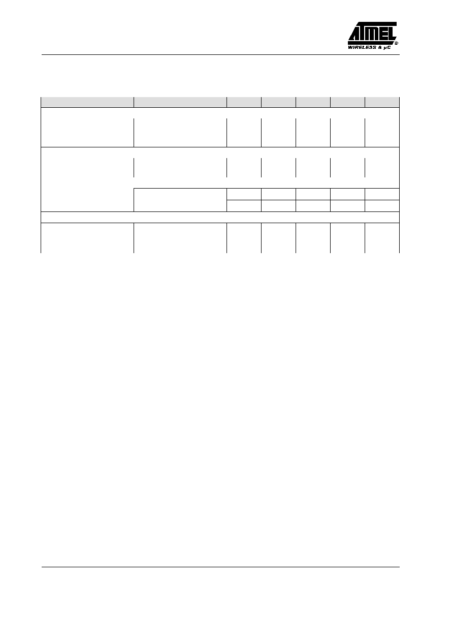
Absolute Maximum Ratings
Reference point Pin 4 (GND), unless otherwise specified
Parameters
Symbol
Value
Unit
Supply current
Pin 8
t
v
10
ms
I
S
i
s
30
150
mA
mA
Output stage
Input voltage
Pin 7
V
I
� 0.5 to V
S
V
Input current
Pin 2, 3
t
v
1 ms
"
I
I
"
I
I
5
30
mA
mA
Input voltage
Pin 5, 6
V
I
0 to V
8
V
Junction temperature
T
j
+125
C
Ambient temperature
T
amb
� 10 to +100
C
Storage temperature range
T
stg
� 40 to +125
C
Thermal Resistance
Parameters
Symbol
Value
Unit
Junction ambient
DIP8
SO8 on p.c.
SO8 on ceramic
R
thJA
R
thJA
R
thJA
110
220
140
K/W
K/W
K/W
Electrical Characteristics
V
S
+ 7 V, T
amb
= 25
�
C, reference point Pin 4 (GND), unless otherwise specified
Parameters
Test Conditions / Pins
Symbol
Min.
Typ.
Max.
Unit
Supply voltage limitation
I
S
+ 3 mA
Pin 8
I
S
+ 30 mA
V
S
V
S
7.2
7.4
8.2
8.4
9.2
9.4
V
V
Current consumption
V
S
+ 7 V
Pin 8
I
S
2
mA
Voltage monitoring
Pin 8
Switch-on threshold
Switch-off threshold
V
Son
V
Soff
5
3
V
V
Synchronization
Pin 3
Voltage limitation
I
3
+1 mA
Pin 3 - 8
I
3
+ �1 mA
V
lim
�V
lim
1.5
0.75
V
V
Switch-on threshold
Switch-off threshold
Pin 3
I
Ton
I
Toff
120
35
mA
mA
Trigger input
Pin 2
Voltage limitation
I
2
+1 mA
Pin 2 - 8
I
2
+ �1 mA
V
lim
�V
lim
1.5
0.75
V
V
Switch-on threshold
Switch-off threshold
Pin 2
I
Ton
I
Toff
120
35
mA
mA
Start delay time
Repetition delay time
f
mains
+ 50 Hz Pin 2-7
t
1
t
2
40
60
60
80
ms
ms
U490B
Rev. A3, 12-Jan-01
4 (6)
Electrical Characteristics (continued)
V
S
+ 7 V, T
amb
= 25
�
C, reference point Pin 4 (GND), unless otherwise specified
Parameters
Test Conditions / Pins
Symbol
Min.
Typ.
Max.
Unit
Phase control
Pin 5, 6, 3
Control input:
Input voltage range
Input current
Pin 5
2 V
v
V
5
v
V
8
V
I
I
I
2
50
90
V
S
130
V
mA
Ramp
Pin 6
Charge current
Discharge current
2V
v
V
6
v
V
8
� 0.5 V
U
5
+ 4 V
I
ch
�I
dis
50
2
90
130
mA
mA
Phase shift
Pin 7-5
C
6
+ 150 nF, V
5
+ 2 V
t
dmax
7
ms
6
,
5
V
5
+ V
8
t
dmin
600
ms
Output stage, V
7
+ 0 V
Pin 7
Output reverse current
Output current
Status OFF
Status ON
"I
o(r)
�I
o
100
10
mA
mA
Pulse width
C
6
+150 nF, see figure 3
t
p
100
200
300
ms