 | –≠–ª–µ–∫—Ç—Ä–æ–Ω–Ω—ã–π –∫–æ–º–ø–æ–Ω–µ–Ω—Ç: U6032B-FP | –°–∫–∞—á–∞—Ç—å:  PDF PDF  ZIP ZIP |
Rev. 4771A≠AUTO≠11/03
Features
∑
Debounce Time: 0.3 ms to 6 s
∑
RC Oscillator Determines Switching Characteristics
∑
Relay Driver with Z-diode
∑
Debounced Input for Toggle Switch
∑
Three Debounced Inputs: ON, OFF and TOGGLE
∑
Load-dump Protection
∑
RF Interference Protection
∑
Protection According to ISO/TR7637-1 (VDE 0839)
Description
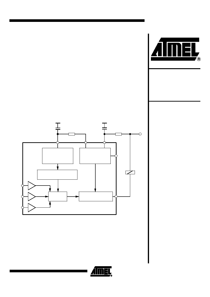
The bipolar integrated circuit U6032B is designed as a toggle switch. The device,
which has a defined power-on status, can be used to control electrical loads, for exam-
ple, fog lamps, high/low beam or heated windows for automotive applications.
Figure 1. Block Diagram with External Circuit
Stabilization
Power-on reset
Load-dump detection
Debouncing
Relay-control output
Oscillator
Frequency divider
ON
OFF
TOGGLE
GND
OSC
6
7
8
3
4
5
1
2
C
2
R
1
510
47 µF
R
2
V
stab
V
S
C
1
V
Batt
Automotive
Toggle Switch
IC
U6032B
2
U6032B
4771A≠AUTO≠11/03
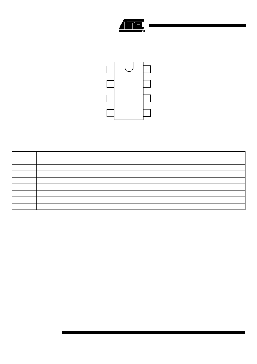
Pin Configuration
Figure 2. Pinning DIP8/SO8
1
2
3
4
8
7
6
5
GND
RELAY
ON
OFF
TOGGLE
OSC
VSTAB
VS
Pin Description
Pin
Symbol
Function
1
GND
Reference point, ground
2
RELAY
Relay control output
3
ON
Switch-on input
4
OFF
Switch-off input
5
TOGGLE
Toggle input
6
OSC
RC oscillator input
7
VSTAB
Stabilized voltage
8
VS
Supply voltage
3
U6032B
4771A≠AUTO≠11/03
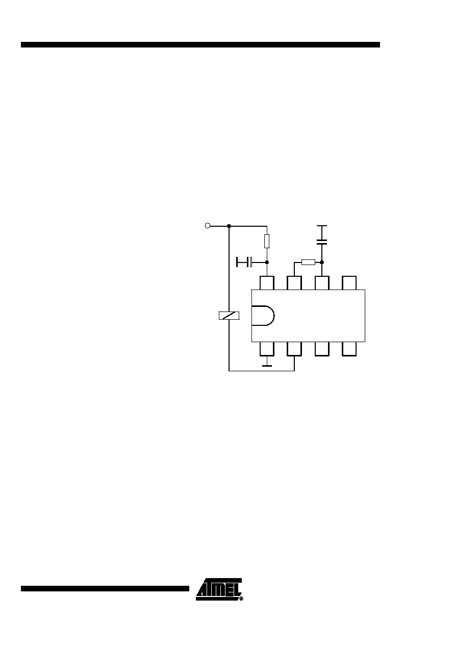
Functional Description
Power Supply, Pin 8
To achieve interference protection and surge immunity, the supply voltage (pin 8) must
be provided with an RC circuit as shown in Figure 3. The dropping resistor, R
1
, limits the
current in case of overvoltage, whereas C
1
smoothes the supply voltage at pin 8.
Recommended values are: R
1
= 510
W
, C
1
= 47 µF.
An integrated Z-diode (14 V) protects the supply voltage, V
S
, thus enabling stable oper-
ation in a supply-voltage range of 6 V to 16 V, supplied by V
Batt
.
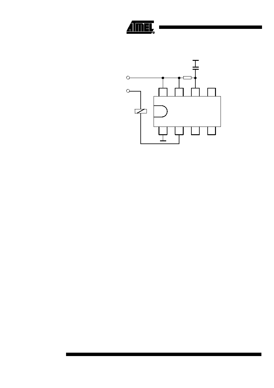
It is possible to operate the integrated circuit with a 5 V supply, but it should be assured
that there are no interference voltages. In this case, pin 7 is connected to pin 8 as shown
in Figure 4 on page 4, and the R
1
C
1
circuit is omitted.
Figure 3. Basic Circuit for 12-V Supply and Oscillator
47 µF/
16 V
510
C
2
1
2
6
5
8
7
3
4
U6032B
R
2
R
1
C
1
V
Batt
4
U6032B
4771A≠AUTO≠11/03
Figure 4. Basic Circuit for V
S
= 5 V
Oscillator, Pin 6
The oscillator frequency, f, is determined mainly by the R
2
C
2
circuit. The resistance, R
2
,
determines the charge time, and the integrated resistance (2 k
W
) is responsible for the
discharge time. To ensure the stability of the oscillator frequency, it is recommended
that the selected R
2
value is remarkably greater than the internal resistance (2 k
W
), as
the temperature response and the tolerances of the integrated resistance are consider-
ably greater than the external resistance value.
The oscillator frequency, f, is calculated as follows:
where
t
1
= charge time =
a
1
¥
R
2
¥
C
2
t
2
= discharge time =
a
2
¥
2 k
W
¥
C
2
a
1
and
a
2
are constants, e.g.:
a
1
= 0.833 and
a
2
= 1.551 when C
2
= 470 pF to 10 nF
a
1
= 0.746 and
a
2
= 1.284 when C
2
= 10 nF to 4700 nF
The debounce time, t
3
, depends on the oscillator frequency, f, as follows:
Table 1 shows the relationship between t
3
, C
2
, R
2
and frequencies from 1 Hz to 20 kHz.
C
2
V
Batt
1
2
6
5
8
7
3
4
V
S
= 5 V
U6032B
R
2
f
1
t
1
t
2
+
---------------
=
t
3
6
1
t
---
¥
=
5
U6032B
4771A≠AUTO≠11/03
Relay-control Output
The relay-control output is an open-collector Darlington circuit with an integrated
23-V Z-diode for limiting the inductive cut-off pulse of the relay coil. The maximum static
collector current must not exceed 300 mA and the saturation voltage is typically 1.1 V at
200 mA.
Interference Voltages
and Load Dump
The lC supply is protected by R
1
, C
1
, and an integrated Z-diode, while the inputs are
protected by a series resistor, integrated Z-diode and RF capacitor (refer to Figure 6 on
page 6).
The relay-control output is protected by the integrated 23 V Z-diode in case of short
interference peaks. It is switched to conductive condition for a battery voltage greater
than 40 V in case of load dump. The output transistor is dimensioned so that it can with-
stand the generated current.
Power-on Reset
When the operating voltage is switched on, an internal power-on reset pulse (POR) is
generated which sets the logic of the circuits to a defined initial condition. The relay out-
put is disabled.
Relay-control Output
Behavior, Pin 2
The time functions (relay output) can be started or interrupted by the three inputs ON,
OFF or TOGGLE (pins 3, 4 and 5, input circuit of these pins see Figure 6 on page 6).
The relay becomes active if the time function is triggered, and the relay contact is inter-
rupted after the elapse of the delay time, t
d
. There are two input possibilities.
Toggle Input, Pin 5
When the push-button (TOGGLE) switch, S
1
, is pressed for the first time, the relay
becomes active after the debounce time, t
3
, i.e., the relay output, pin 2, is active.
Repeated operation of S
1
causes the interruption of the relay contact, thus disabling the
relay. Each operation of the toggle switch, S
1
, changes (alters) the condition of the relay
output when the debounce time, td, is exceeded, i.e., the TOGGLE function.
If the relay output is not disabled by pressing the switch S
1
, the output stays active.
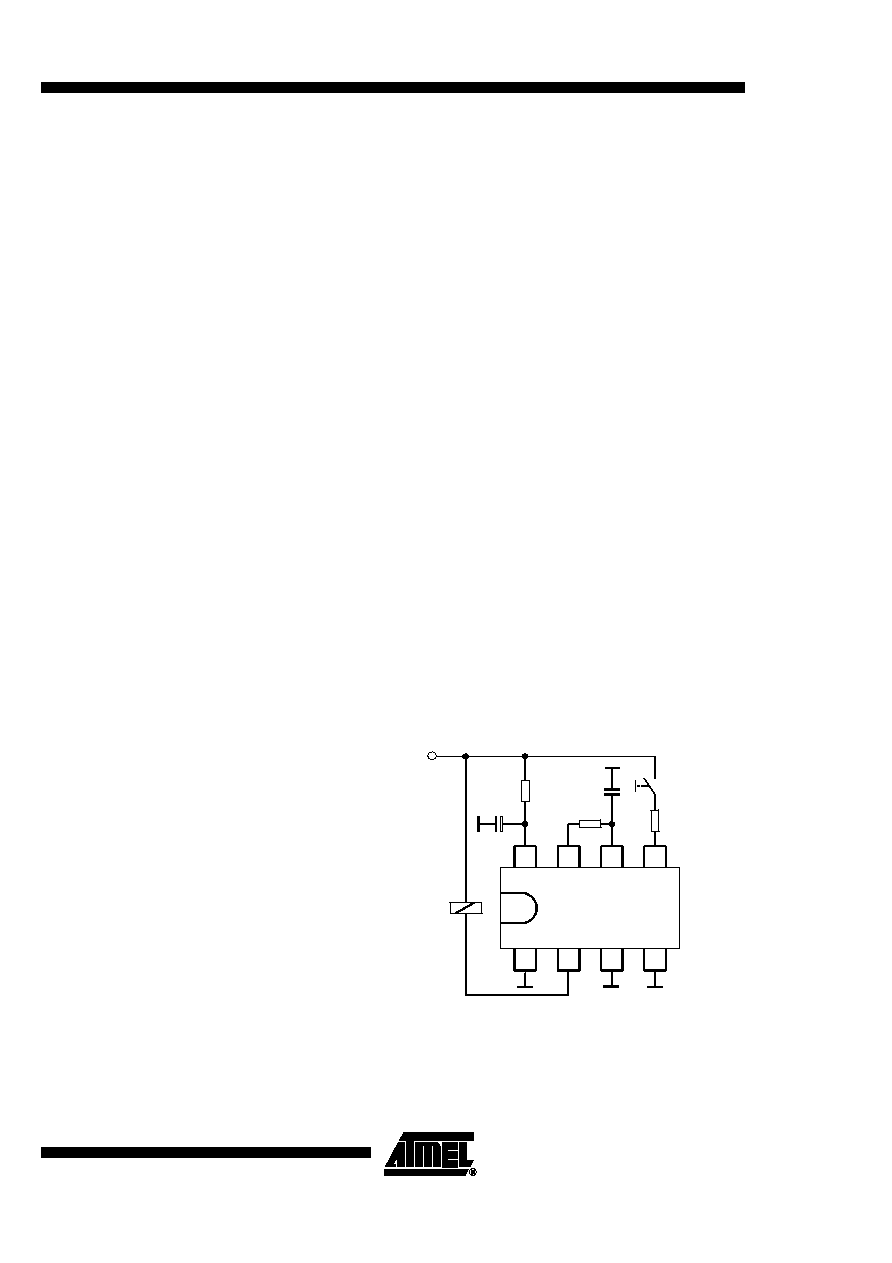
Figure 5. TOGGLE Function
47 µF/
16 V
510
R
2
C
2
V
Batt
1
2
6
5
8
7
3
4
20 k
S
1
U6032B
R
1
C
1