Rev. 4810A≠AUTO≠03/04
Features
∑
Temperature and Voltage Compensated Frequency
∑
Warning Indication of Lamp Failure by Means of Frequency Doubling can be Disabled
∑
Voltage Dependence of the Car Indicator Lamps Compensated for Lamp Failure
∑
Relay Output with High Current Carrying Capacity and Low Saturation Voltage
∑
Minimum Lamp Load for Flasher Operation
1 W
∑
Load-dump Protection
∑
Very Low Susceptibility to EMI
∑
Protection According to ISO/TR 7637/1 Level 4
Description
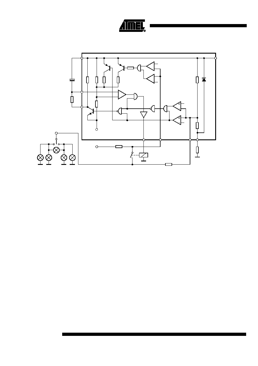
The design of the U6433B is similar to that of U6043B, both devices have the same
excellent EMC (Electro Magnetic Capability) and protection features. The U6433B
includes an additional 8-mV comparator and a logical connection with the frequency
doubling stage. This combination can be used for a hazard switch which bypasses the
external shunt resistor to disable the frequency doubling. This feature is especially
important with respect to the US automotive industry. During direction mode the
U6433B works like other flashers, i.e., frequency doubling in the case of lamp outage.
Flasher, 18-m
Shunt,
Frequency
Doubling
Disabling
U6433B

4
U6433B
4810A≠AUTO≠03/04
Functional Description
Pin 1, GND
The integrated circuit is protected against damage via resistor R
4
to ground (-31) in the
case of battery reversal.
An integrated protection circuit together with external resistances R
2
and R
4
limits the
current pulses in the IC.
Pin 2, Supply Voltage,
V
S
- Power
The arrangement of the supply connections to pin 2 must be so as to ensure that, on the
connection printed circuit board (PCB), the resistance of V
S
to pin 6 is lower than that to
pin 2.
Pin 3, Relay Control
Output (Driver)
The relay control output is a high-side driver with a low saturation voltage and is capable
of driving a typical automotive relay with a minimum coil resistance of 60
.
Pin 4 and 5 Oscillator
The flashing frequency, f
1
, is determined by the R
1
C
1
components as follows (see Fig-
ure 1 on page 2):
where
C
1
47 µF
R
1
+ 6.8 k
to 510 k
In the case of a lamp outage (see pin 7) the oscillator frequency is switched to the lamp
outage frequency f
2
with f
2
2.2 f
1
.
Duty cycle in normal flashing mode: 50%
Duty cycle in lamp outage mode: 40% (bright phase)
Pin 6, Supply Voltage,
Sense
For accurate monitoring via the shunt resistor, a minimized layer resistance from point
V
S
/shunt to pin 6 is recommended.
Pin 7, Lamp outage
detection
Control Signal Threshold 1
(49-mV Comparator K1)
The detection point for lamp failure can be calculated from the control signal threshold,
typically 49 mV with V
S
= 12 V. With a measuring resistance of R
3
= 18 m
, the fre-
quency change-over is reached at a lamp load of 21 W + 11.4 W. The variation of the
control signal threshold supply voltage takes into account the PTC characteristic of fila-
ment lamps.
Control Signal Threshold 2
(8-mV Comparator K4)
A voltage drop between 49 mV to 8 mV at R
3
shunt resistor lets the flasher work in fre-
quency doubling mode.
If the voltage drop decreases to a value below V
R3MAX
= 8 mV, frequency doubling is dis-
abled. This can be achieved either with a switch which bypasses the shunt resistor (e.g.,
a special hazard warning switch) or with a small lamp load.
f
1
1
R
1
C
1
◊
1.5
◊
-------------------------------------
Hz
5
U6433B
4810A≠AUTO≠03/04
The arrangement of the supply connections to pins 2 and 6 must ensure that, on the
connection PCB, the layer resistance from V
S
to pin 6 is lower than the one to pin 2.
Flasher operation starts with a lamp load of P
L
1 W.
Pin 8, Start Input
Start condition for flashing: the voltage at pin 8 has to be below K3 threshold (flasher
switch closed).
Humidity and dirt may decrease the resistance between 49 a and GND. If this leakage
resistance is > 5 k
the IC is still kept in its offcondition. In this case the voltage at pin 8
is between the thresholds of comparators K2 and K3.
During the bright phase the voltage at pin 8 is above the K2 threshold, during the dark
phase it is below the K3 threshold.
For proper start conditions a minimum lamp wattage of 1 W is required.
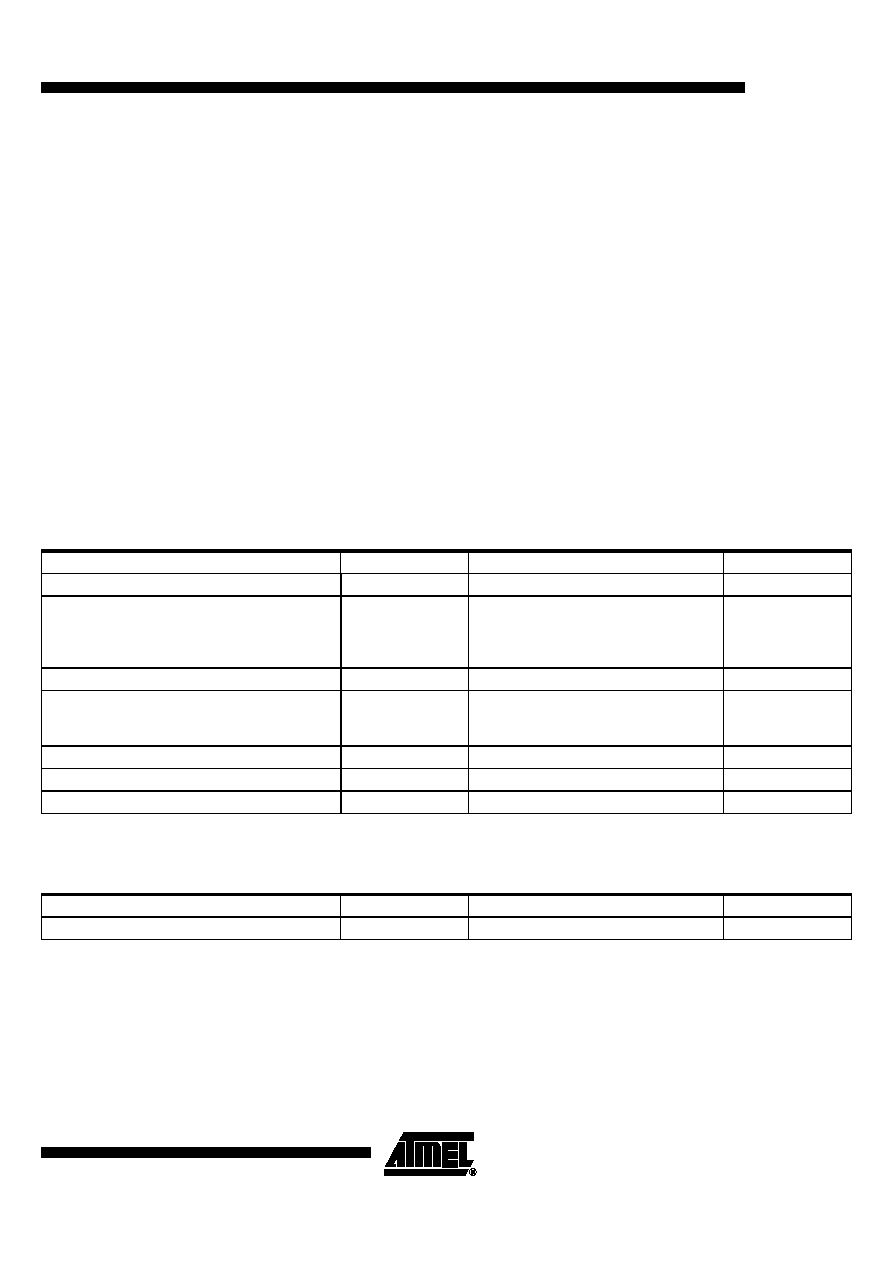
Absolute Maximum Ratings
Stresses beyond those listed under "Absolute Maximum Ratings" may cause permanent damage to the device. This is a stress rating
only and functional operation of the device at these or any other conditions beyond those indicated in the operational sections of this
specification is not implied. Exposure to absolute maximum rating conditions for extended periods may affect device reliability.
Reference point pin 1.
Parameters
Symbol
Value
Unit
Supply voltage, pins 2 and 6
V
S
18
V
Surge forward current
t
p
= 0.1 ms, pins 2 and 6
t
p
= 300 ms, pins 2 and 6
t
p
= 300 ms, pin 8
I
FSM
1.5
1.0
30.0
A
A
mA
Output current, pin 3
I
O
0.3
A
Power dissipation
T
amb
= 95∞C, SO8
T
amb
= 60∞C, SO8
P
tot
340
560
mW
mW
Junction temperature
T
j
150
∞C
Ambient temperature range
T
amb
-40 to +105
∞C
Storage temperature range
T
stg
-55 to +150
∞C
Thermal Resistance
Parameters
Symbol
Value
Unit
Junction ambient SO8
R
thJA
160
K/W