 | –≠–ª–µ–∫—Ç—Ä–æ–Ω–Ω—ã–π –∫–æ–º–ø–æ–Ω–µ–Ω—Ç: U6808B | –°–∫–∞—á–∞—Ç—å:  PDF PDF  ZIP ZIP |
1
Features
∑
Digital Self-supervising Watchdog with Hysteresis
∑
One 250-mA Output Driver for Relay
∑
Enable Output Open Collector 8 mA
∑
Over/Undervoltage Detection
∑
ENABLE and RELAY Outputs Protected Against Standard Transients
and 40 V Load Dump
∑
ESD Protection According to MIL-STD-883 D Test Method 3015.7
≠ Human Body Model: ±2 kV (100 pF, 1.5 k
W
)
≠ Machine Model: ±200 V (200 pF, 0
W
)
Description
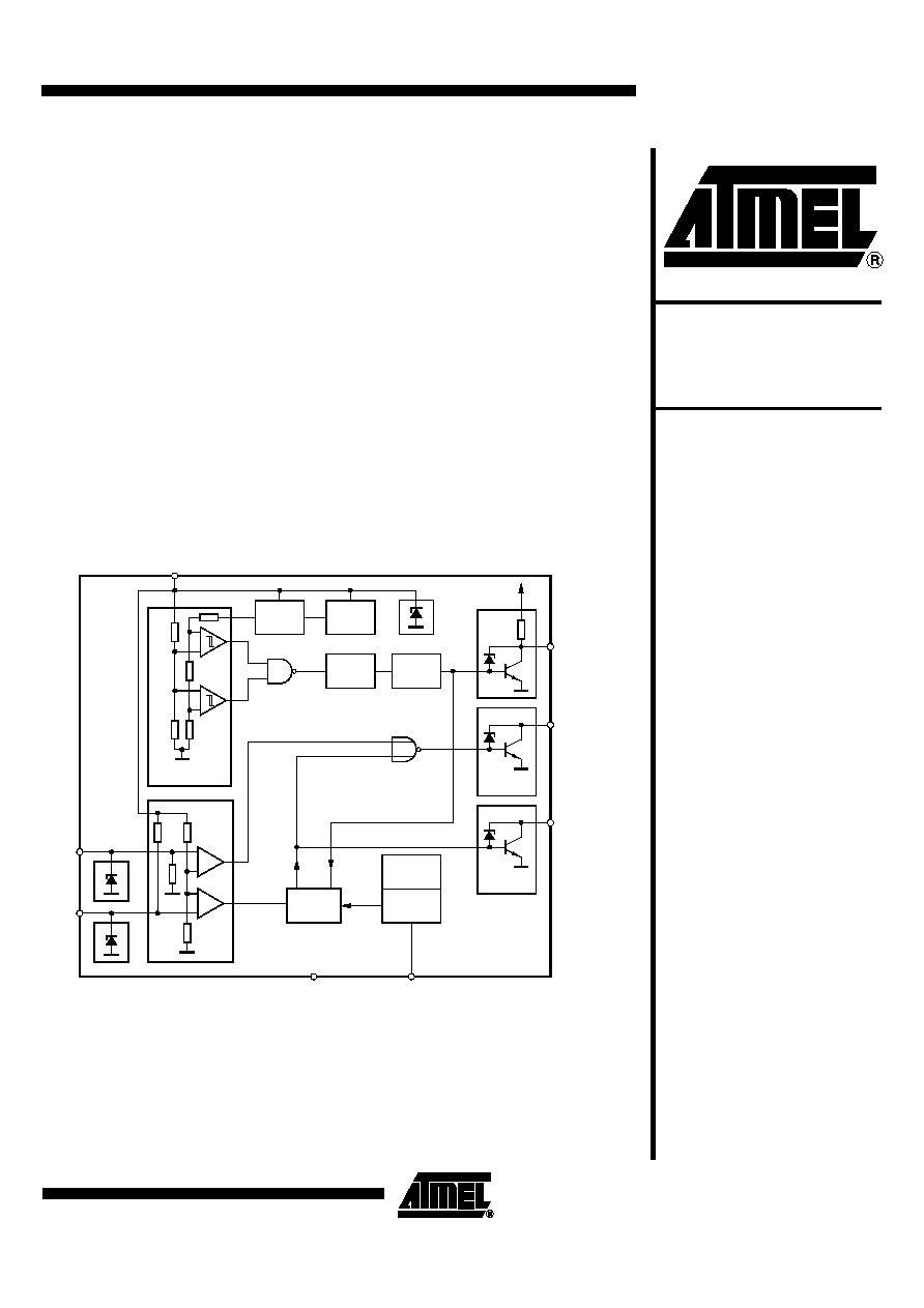
The U6808B is designed to support the fail-safe function of a safety critical system
(e.g., ABS). It includes a relay driver, a watchdog controlled by an external R/C-net-
work and a reset circuit initiated by an over and undervoltage condition of the 5-V
supply providing a low-level reset signal.
Figure 1. Block Diagram
Bandgap
reference
2.44 V
+
-
+
-
Under/ overvoltage
detection
Reset
debounce
Power-on
reset
Reset
delay
-
+
+
-
Current
limitation
Internal
oscillator
RC
oscillator
Watchdog
V
S
RIN
WDI
WDC
GND
RESET
RELAY
ENABLE
V
S
Special
Fail-safe IC
U6808B
Rev. 4707A≠AUTO≠05/03

2
U6808B
4707A≠AUTO≠05/03
Pin Configuration
Figure 2. Pinning SO8
Fail-safe Functions
A fail-safe IC has to maintain its monitoring function even if there is a fault condition at
one of the pins (e.g., short circuit). This ensures that a microcontroller system is not
brought into a critical status. A critical status is reached if the system is not able to
switch off the relay and to give a signal to the microcontroller via the ENABLE and
RESET outputs. The following table shows the fault conditions for the pins.
Table 1. Table of Fault Conditions
1
2
3
4
8
7
6
5
RELAY
GND
ENABLE
WDC
VS
RIN
WDI
RESET
Pin Description
Pin
Symbol
Type
Function
Logic
1
RELAY
Open collector
driver output
Fail-safe relay driver
No signal: driver off
Low: driver on
2
GND
Supply
Standard ground
No signal
3
ENABLE
Digital output
Negative reset signal
Low: reset
4
WDC
Analog input
External RC for watchdog timer
No signal
5
RESET
Digital output
Negative reset signal
Low: reset
6
WDI
Digital input
Watchdog trigger signal
Pulse sequence
7
RIN
Digital input
Activation of relay driver
High: driver on
Low: driver off
8
VS
Supply
5-V supply
≠
Pin
Function
Short to Vs
Short to VBat
Short to GND
Open Circuit
RIN
Digital input to
activate the fail-safe
relay
Relay on
Relay on
Relay off
Relay off
WDI
Watchdog trigger
input
Watchdog reset
Watchdog reset
Watchdog reset
Watchdog reset
OSC
Capacitor and
resistor of watchdog
Watchdog reset
Watchdog reset
Watchdog reset
Watchdog reset
RELAY
Driver of the fail-safe
relay
Relay on
Relay off

3
U6808B
4707A≠AUTO≠05/03
Truth Tables
Table 2. Truth Table for Over and Undervoltage Conditions
Table 3. Truth Table for Watchdog Failures (Reset Output Do Not Care)
Description of the Watchdog
Figure 3. Watchdog Block Diagram
Abstract
The microcontroller is monitored by a digital window watchdog which accepts an incom-
ming trigger signal of a constant frequency for correct operation. The frequency of the
trigger signal can be varied in a broad range as the watchdog's time window is deter-
mined by external R/C components. The following description refers to the block
diagram, see Figure 3.
Supply Voltage
(V
S
)
Relay Input
(RIN)
Relay Output
Driver (RELAY)
RESET Output
(RESET)
Enable Output
Driver (ENABLE)
Normal
Low
Off
High
Off
High
On
High
Off
Too low
Low
Off
Low
On
High
Off
Low
On
Too high
Low
Off
Low
On
High
Off
Low
On
Watchdog Input
(WDI)
Relay Input
(RIN)
Relay Output Driver
(RELAY)
Enable Output Driver
(ENABLE)
Normal
Low
Off
Off
High
On
Off
Too slow
Low
Off
On
High
Off
On
Too fast
Low
Off
On
High
Off
On
Slope
detector
Up/down
counter
Dual MUX
Binary counter
RS-FF
RCOSC
WDI
RESET
OSCERR
WD-OK
4
U6808B
4707A≠AUTO≠05/03
WDI Input
The microcontroller has to provide a trigger signal with the frequency f
WDI
which is fed to
the WDI input. A positive edge of f
WDI
detected by a slope detector resets the binary
counter and clocks the up/down counter additionally. The latter one counts only from
0 to 3 or reverse. Each correct trigger increments the up/down counter by 1, each wrong
trigger decrements it by 1. As soon as the counter reaches status 3 the RS flip-flop is set
(see Figure 4). A missing incoming trigger signal is detected after 250 clocks of the inter-
nal watchdog frequency f
RC
(see section "WD-OK Output") and resets the up/down
counter directly.
RCOSC Input
With an external R/C circuitry the IC generates a time base (frequency f
WDC
) indepen-
dent from the microcontroller. The watchdog's time window refers to a frequency of
f
WDC
= 100
¥
f
WDI
OSCERR Input
A smart watchdog has to ensure that internal problems with its own time base are
detected and do not lead to an undesired status of the complete system. If the RC oscil-
lator stops oscillating a signal is fed to the OSCERR input after a timeout delay. It resets
the up/down counter and disables the WD-OK output.
Without this reset function the watchdog would freeze in its current status when f
RC
stops.
RESET Input
During power-on and under/overvoltage detection a reset signal is fed to this pin. It
resets the watchdog timer and sets the initial state.
WD-OK Output
After the up/down counter is incremented to status 3 (see Figure 4) the RS flip-flop is set
and the WD-OK output becomes logic 1. This information is available for the microcon-
troller at the open-collector output ENABLE. If on the other hand the up/down counter is
decremented to 0 the RS flip-flop is reset, the WD-OK output and the ENABLE output
are disabled. The WD-OK output also controls a dual MUX stage which shifts the time
window by one clock after a successful trigger, thus forming a hysteresis to provide sta-
ble conditions for the evaluation of the trigger signal good or false. The WD-OK signal is
also reset in case the watchdog counter is not reset after 250 clocks (missing trigger
signal).
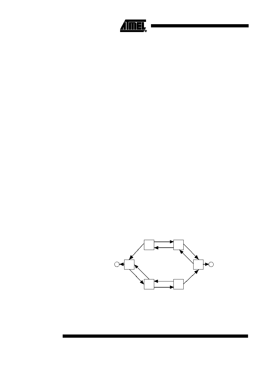
Watchdog State Diagram
Figure 4. Watchdog State Diagram
1/NF
2/NF
O/F
1/F
2/F
3/NF
bad
good
bad
good
bad
good
good
bad
good
good
bad
bad
Initial status

5
U6808B
4707A≠AUTO≠05/03
Explanation
In each block, the first character represents the state of the counter. The second nota-
tion indicates the fault status of the counter. A fault status is indicated by an F and a no
fault status is indicated by an NF. When the watchdog is powered up initially, the
counter starts out at the 0/F block (initial state). Good indicates that a pulse has been
received whose width resides within the timing window. Bad indicates that a pulse has
been received whose width is either too short or too long.
Watchdog Window
Calculation
Example with Recommended
Values
C
osc
= 3.3 nF (should be preferably 10%, NPO)
R
osc
= 39 k
W
(may be 5%, Rosc < 100 k
W
due to leakage current and humidity)
RC Oscillator
t
WDC
(s) = 10
-3
¥
[C
osc
(nF)
¥
[(0.00078
¥
R
osc
(k
W
)) + 0.0005]]
f
WDC
(Hz) = 1/(t
WDC
)
Watchdog WDI
f
WDI
(Hz) =0.01
¥
f
WDC
t
WDC
= 100 µs
Æ
f
WDC
= 10 kHz
f
WDI
= 100 Hz
Æ
t
WDI
= 10 ms
WDI Pulse Width for Fault
Detection after 3 Pulses
Upper watchdog window
Minimum: 169/f
WDC
= 16.9 ms
Æ
f
WDC
/169 = 59.1 Hz
Maximum: 170/f
WDC
= 17.0 ms
Æ
f
WDC
/170 = 58.8 Hz
Lower watchdog window
Minimum: 79/f
WDC
= 7.9 ms
Æ
f
WDC
/79 = 126.6 Hz
Maximum: 80/f
WDC
= 8.0 ms
Æ
f
WDC
/80 = 125.0 Hz
WDI Dropouts for Immediate
Fault Detection
Minimum: 250/f
WDC
= 25 ms
Maximum: 251/f
WDC
= 25.1 ms
Figure 5. Watchdog Timing Diagram with Tolerances
Reset Delay
The duration of the over or undervoltage pulses determines the enable and reset output.
A pulse duration shorter than the debounce time has no effect on the outputs. A pulse
longer than the debounce time results in the first reset delay. If a pulse appears during
this delay, a second delay time is triggered. Therefore, the total reset delay time can be
longer than specified in the data sheet.
Time/s
79/f
WDC
80/f
WDC
169/f
WDC
170/f
WDC
250/f
WDC
251/f
WDC
Watchdog window
update rate is good
Update rate is too
fast
Update rate is
either too fast or
good
Update rate is
either too slow or
good
Update rate is too
slow
Update rate is
either too slow or
pulse has
dropped out
Pulse has
dropped out