 | –≠–ª–µ–∫—Ç—Ä–æ–Ω–Ω—ã–π –∫–æ–º–ø–æ–Ω–µ–Ω—Ç: U6812B | –°–∫–∞—á–∞—Ç—å:  PDF PDF  ZIP ZIP |
Rev. 4760A≠AUTO≠10/03
Features
∑
Wide Power Supply Voltage Range
∑
Short-circuit Protected K-interface, ISO9141 Compatible
∑
Three Short-circuit Protected 40-mA Open-collector Buffers
∑
All Low-power Outputs with Built-in 28-V Clamping
∑
CMOS Compatible Digital Inputs with Hysteresis
∑
Digital 1-mA Push-pull "RxD" K-line Output
∑
Channel-specific Over-temperature Switch Off in Event of Short Circuit
∑
Load-dump Protection and Interference Protection
According to ISO 7637-1/4 (DIN 40839)
Description
The U6812B is a bipolar monolithic K-line bus transceiver designed to provide
bi-directional serial communication in automotive diagnostic applications. The stan-
dard K-line is ISO 9141 compatible for baud rates up to 250 kBaud.
The IC provides three universally applicable 40-mA open-collector buffers, that can be
used for signal decoupling. The U6812B is manufactured using Atmel's bipolar pro-
cess and fully complies to automotive industry specifications.The U6812B provides an
ideal grouping of SO-packaged low-power drivers, thus meeting customers' demand
for space-saving and cost-effective circuit board assembly.
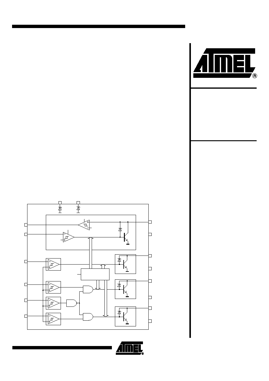
Figure 1. Block Diagram
VCC/2
K
IN 1
IN 2
DIS
IN 3
VS
VCC
TXD
TXD
OUT 1
GND
OUT 2
GND
OUT 3
Temperature
control
VCC
VS/2
VCC/2
K-diagnosis ISO 9141
VCC
VS
GND
GND
Single-ended
Bus Transceiver
with Triple
Buffer
U6812B
2
U6812B
4760A≠AUTO≠10/03
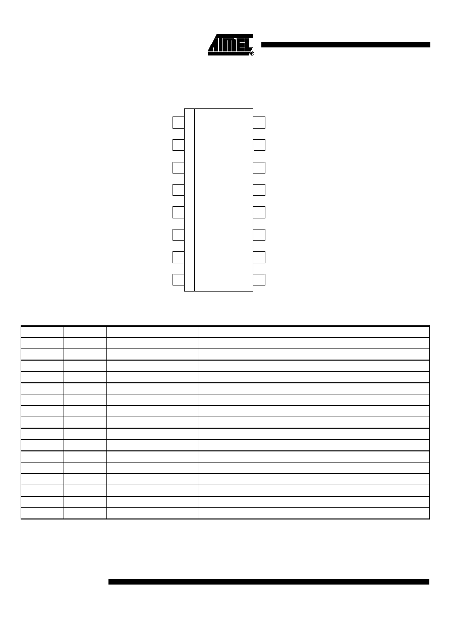
Pin Configuration
Figure 2. Pinning SO16
1
2
3
4
5
6
7
8
16
15
14
13
12
11
10
9
IN 2
DIS
VCC
IN 3
OUT 3
GND
GND
OUT 2
TXD
RXD
VS
IN 1
OUT 1
GND
GND
K
U6812B
Pin Description
Pin
Symbol
Type
Function
1
GND
Supply
Ground; all ground pins are directly connected to the lead frame
2
OUT 2
Open-collector output
Protected output of driver 2 (faced to: outside)
3
IN 2
Digital input
Input of protected driver 2 (faced to: µP)
4
DIS
Digital input
Disable input for OUT 2 and OUT 3, "H"=enable, "L"=disable
5
VCC
Supply
+5-V supply
6
IN 3
Digital input
Input of protected driver 3 (faced to: µP)
7
OUT 3
Open-collector output
Protected output of driver 3 (faced to: outside)
8
GND
Supply
Ground
9
GND
Supply
Ground
10
OUT 1
Open-collector output
Protected output of driver 1 (faced to: outside)
11
IN 1
Digital input
Input of protected driver 1 (faced to: µP)
12
VS
Supply/reference
+12-V reference for K-line level
13
RXD
Digital output
Diagnosis receive line (faced to: µP)
14
TXD
Digital input
Diagnosis transmit line (faced to: µP)
15
K
12-V input and O.C. output
Bi-directional diagnosis line (faced to: outside)
16
GND
Supply
Ground
3
U6812B
4760A≠AUTO≠10/03
Figure 3.
Basic Application Circuit
1
2
3
4
5
6
7
8
16
15
14
13
12
11
10
9
OUT 3
OUT 2
OUT 1
RXD
K
V
Batt
TXD
IN 1
IN 2
IN 3
VCC
DIS
10 µ
1k
V
S
U6812B
+
C
2
R
1
C
1
D
1

4
U6812B
4760A≠AUTO≠10/03
Functional Description
K-interface
The K-interface is equipped with a 40-mA open-collector driver. The current is deter-
mined by the external pull-up resistor. The saturation voltage is below 0.6 V.
The open-collector output is protected by a 28-V Z-diode. The collector current is per-
manently monitored for short circuits via a built-in shunt. In the event of a short circuit
occurring at V
Batt
, the collector current is held at approximately I
creg
= 80 mA; the chip
temperature then rises due to power loss. This status is maintained until the detection of
overtemperature which causes the K-line output to be disabled and stored to memory.
The internal short-circuit detection threshold is I
sc
> 0.8
¥
I
creg
. The output remains dis-
abled until a falling edge of a pulse is available to its input. Any further attempt to
connect while the short circuit is still present causes the above sequence to be
repeated. The output can be activated normally once the short circuit has been
removed. The maximum baud rate is 250 kBaud.
The K-line allows bi-directional communication with the microcontroller. When the out-
put K is disabled, information can be transferred to the processor via the input
comparator at pin RxD.
The digital output RxD is a push-pull output stage with a driver power of 1 mA.
In the event of a line break at the K-line, the output K is connected to GND via the built-
in 85-k
W
pull-down resistor, thus allowing the microcontroller to detect this fault. The
maximum sampling frequency is 250 kBaud.
Open-collector Driver
OUTx
The outputs are designed for a maximum static current of 40 mA, which is determined
by the external pull-up resistor. The saturation voltage is below 0.6 V
The three OUTx-driver outputs are activated with "active low" at the corresponding
input. Outputs OUT2 and OUT3 can also be disabled with "active low" at the disable
input, regardless of their input signal. The outputs are released by an open disable input
or by using high potential.
The open-collector outputs are connected to a 28-V Z-diode. The collector current is
permanently monitored via a built-in shunt circuit to permit the detection of short circuits.
If a short circuit occurs at V
Ba tt
, the collector current is held at approximately
I
creg
= 80 mA; accompanied with a rise of chip temperature due to power loss. This sta-
tus is maintained until the detection of overtemperature which causes the output
affected by the short circuit to be selectively disabled and stored to memory. The inter-
nal short-circuit detection threshold is I
sc
> 0.8
¥
I
creg
. The affected output remains
disabled until a falling edge of a pulse is available to its input. Any further attempt to con-
nect while the short circuit is still present causes the above sequence to be repeated.
The output can be activated normally once the short circuit has been removed.
Power Supply
The IC must be equipped with external RC circuitry to limit the voltage in the event of
power surges (see Figure 3 on page 3). This prevents the circuit from being damaged or
destroyed, and provides a buffer in case of power fluctuations at V
Batt
. The RxD compar-
ator is powered via pin V
S
, producing its reference voltage of 1/2 V
S
, while all other
blocks are supplied via V
CC
.
The operating voltage can vary between V
S
= 7 V and 26 V. The resistor R
1
at pin V
S
lim-
its the current via the built-in 28-V Z-diode between V
S
and GND.
5
U6812B
4760A≠AUTO≠10/03
Application Note
It is recommended to use the external components as shown in Figure 3 on page 3 with
the reverse battery protection diode D
1
and the buffer capacitor C
1
= 10 µF.
Digital Inputs (DIS, IN 1,
IN 2, IN 3 and TxD)
The digital inputs are CMOS-compatible and equipped with a built-in pull-up resistor
with a typical rating of 85 k
W
to V
CC
. The input threshold totals V
TH
= 0.57
¥
V
CC
with a
typical hysteresis of 100 mV. The inputs are designed for an input voltage of -0.2 V to
V
CC
+ 0.6 V.
For proper activation of the output stages, it is mandatory that the inputs are kept low as
long as the supply voltage is not applied. When the supply voltage has been applied, all
inputs need to have a falling edge (see "Timing Diagrams" on page 6).
Digital Output (RxD)
The digital output RxD is a push-pull output stage with a driver power of I
RxD
= 1 mA.
Interference Voltages
and Load Dump (Defined
in DIN40839 or ISO7637)
The U6812B is protected against interference pulses (usually present in the wiring) by
the recommended R
1
C
1
circuitry and the integrated elements (28-V Z-diodes, both at
the supply pin and at the output pins and two diodes connected to V
CC
and GND at the
digital inputs). All transient pulses, which appear on the supply line (V
Batt
), should not
affect the function of the IC (see Table 1).
Table 1.
Transient Test Conditions
Name
Voltage
Source Resistance
Rise Time
Pulse Duration
Pulse Amount
DIN/ISO 1
-110 V
10
W
100 V/µs
2 ms
15000
DIN/ISO 2
110 V
10
W
100 V/µs
0.05 ms
15000
DIN/ISO 3a
-160 V
50
W
30 V/ns
0.1 µs
1 h (reference to ISO)
DIN/ISO 3b
150 V
50
W
20 V/ns
0.1 µs
1 h (reference to ISO)
DIN/ISO 5
55 V (total)
2
W
10 V/ms
500 ms
20
Table 2.
Truth Table
WSI-1
WSI-2
WSI-R
EN
TXD
K
WSO-1
WSO-2
WSO-R
RXD
L
L
X
H
X
X
L
L
X
X
H
H
X
X
X
X
Open
Open
X
X
L
L
X
L
X
X
Open
Open
X
X
X
X
H
X
H
Open
X
X
Open
H
X
X
L
X
L
L
L
X
L
L
X
X
X
X
X
H
X
X
X
H