 | –≠–ª–µ–∫—Ç—Ä–æ–Ω–Ω—ã–π –∫–æ–º–ø–æ–Ω–µ–Ω—Ç: U6813B | –°–∫–∞—á–∞—Ç—å:  PDF PDF  ZIP ZIP |
1
Features
∑
Digital Self-supervising Watchdog with Hysteresis
∑
One 150-mA Output Driver for Relay
∑
One High-side Driver for N-channel Power FET
∑
Positive and Negative Enable Output
∑
Positive and Negative Reset Output
∑
Over/Under-voltage Detection
∑
Relay and Power FET Outputs Protected Against Standard Transients and 55-V Load
Dump
Description
The function of microcontrollers in safety-critical applications (e.g., anti-lock systems)
needs to be monitored permanently. Usually, this task is accomplished by an indepen-
dent watchdog timer. The monolithic IC U6813B, designed in bipolar technology and
qualified according to the needs of the automotive industry, includes such a watchdog
timer and provides additional features for added value. With the help of integrated
driver stages, it is easy to control safety-related functions of a relay and of an N-chan-
nel power MOSFET in high-side applications. In case of a microcontroller malfunction
or supply-voltage anomalies, the U6813B provides positive and negative reset and
enable output signals. This flexibility guarantees a broad range of applications. The
U6813B is based on of Atmel's fail-safe ICs U6808B and U6809B.
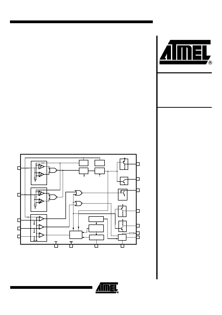
Figure 1. Block Diagram
3.3 V
RELI
FETI
WDI
WDC
CAPI
P-EN
N-EN
RELO
N-RES
P-RES
5-V under- and
overvoltage detect.
3.3-V under- and
overvoltage detect.
Watchdog
19k
19k
19k
V
CC
Reset
debounce
Reset
delay
Power-on
reset
Bandgap
reference
2.44 V
FET
output
Internal
oscillator
RC-
oscillator
supervisor
RC
oscillator
fosc
fosc
FETO
GND
SGND
fosc
16
14
13
12
11
15
2
10
8
7
9
5
6
1
4
3
V
CC
V
CC
Current
limitation
V
S
V
CC
Fail-safe IC with
High-side and
Relay Driver
U6813B
Rev. 4543A≠AUTO≠05/02
2
U6813B
4543A≠AUTO≠05/02
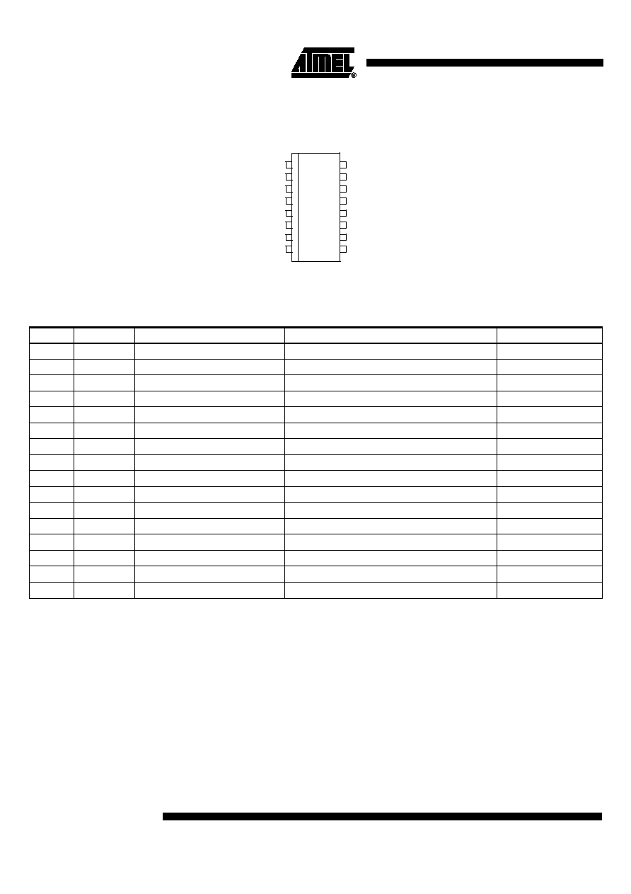
Pin Configuration
Figure 2. Pinning SO16
Fail-safe Functions
A fail-safe IC has to maintain its monitoring function even if there is a fault condition at
one of the pins (e.g., short circuit), ensuring that a microcontroller system does not
reach a "critical status". A critical status means, for example, if the system is not able to
switch off the relay or disable the power MOSFET, or if the system is not able to provide
a signal to the microcontroller via ENABLE- and RESET-outputs in the case of a fault
condition. The U6813B is designed to handle those fault conditions according to Table 1
for a maximum of system safety.
1
2
3
4
5
6
7
8
16
15
14
13
12
11
10
9
RELO
GND
P-RES
N-RES
P-EN
N-EN
V
S
CAPI
3.3V
SGND
V
CC
RELI
FETI
WDI
WDC
FETO
Pin Description
Pin
Symbol
Description
Function
Type
1
RELO
Open-collector output driver
Fail-safe relay driver
Driver on: L
2
GND
Supply
General ground
3
P-RES
Digital output
Positive reset signal
Reset: H
4
N-RES
Digital output
Negative reset signal
Reset: L
5
P-EN
Digital output
Positive enable signal
Enable: H
6
N-EN
Digital output
Negative enable signal
Enable: L
7
V
S
Battery supply
Voltage for charge pump
8
CAPI
Analog input
Input bootstrap capacitor
9
FETO
Power FET output
High voltage for N-channel FET
10
WDC
Analog input
External RC for watchdog timer
11
WDI
Digital input
Watchdog trigger signal
Pulse sequence
12
FETI
Digital input
Activation of power FET
FET on: H
13
RELI
Digital input
Activation of relay driver
Driver on: H
14
V
CC
Supply
5-V supply
15
SGND
Supply
Sense ground, reference for V
CC
and 3.3 V
16
3.3V
Analog input
3.3-V supply
3
U6813B
4543A≠AUTO≠05/02
Table 1. Truth Table
Notes: 1. default state at open input
2. P-EN disable: low
3. N-EN disable: high
Watchdog Description
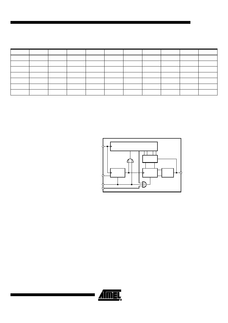
Figure 3. Watchdog Block Diagram
The microcontroller is monitored by a digital window watchdog which accepts an incom-
ming trigger signal of a constant frequency for correct operation. The frequency of the
trigger signal can be varied in a broad range as the watchdog's time window is deter-
mined by external R/C components. The following description refers to the watchdog
timing diagram with tolerances (see Figure 4).
WDI Input (Pin 11)
The microcontroller has to provide a trigger signal with the frequency f
WDI
which is fed to
the WDI input. A positive edge of f
WDI
detected by a slope detector resets the binary
counter and clocks the up/down counter.The latter one counts only from 0 to 3 or
reverse. Each correct trigger increments the up/down counter by 1, each wrong trigger
decrements it by 1. As soon as the counter reaches status 3, the RS flip-flop is set; see
Figure 5 (Watchdog state diagram). A missing incoming trigger signal is detected after
250 clocks of the internal watchdog frequency f
RC
(see WD_OK output) and resets the
up/down counter directly.
WDC Input (Pin 10)
It is to be equiped by external R/C components. By means of an external R/C circuitry,
the IC generates a time base (frequency f
WDC
) independent from the microcontroller.
The watchdog's time window refers to a frequency of f
WDC
= 100
¥
f
WDI
.
VCC
3.3V
WDI
RELI
FETI
RELO
FETO
N-RES
P-RES
P-EN
(2)
N-EN
(3)
ok
ok
ok
H
x
on x
H
L
H
L
ok
ok
ok
L
(1)
x
off
x
H
L
H
L
ok
ok
ok
x
H x
on
H
L
H
L
ok
ok
ok
x
L
(1)
x
off
H
L
H
L
ok
ok
wrong
x
x
off
off
H
L
L
H
x
wrong
x
x
x
off
off
L
H
L
H
wrong
x
x
x
x
off
off
L
H
L
H
Slope
detector
Up/down
counter
Dual MUX
Binary counter
RS-FF
WDC
WDI
RESET
OSCERR
WD-OK
4
U6813B
4543A≠AUTO≠05/02
OSCERR Input
A smart watchdog has to ensure that internal problems with its own time base are
detected and do not lead to an undesired status of the complete system. If the RC oscil-
lator stops oscillating, a signal is fed to the OSCERR input after a timeout delay. It
resets the up/down counter and disables the WD-OK output. Without this reset function,
the watchdog would freeze its current status when f
RC
stops.
RESET Input
During power-on and under/overvoltage detection, a reset signal is fed to this pin. It
resets the watchdog timer and sets the initial state.
WD-OK Output
After the up/down counter has reached to status 3 (see Figure 5, Watchdog State
Diagram), the RS flip-flop is set and the WD-OK output becomes logic "1". As WD-OK is
directly connected to the enable pins, the open-collector output P-EN provides also logic
"1" while a logic "0" is available at N-EN output. If on the other hand the up/down counter
is decremented to "0", the RS flip-flop is reset, the WD-OK output and the P-EN output
are logic "0" and N-EN output is logic "1". The WD-OK output also controls a dual MUX
stage which shifts the time window by one clock after a successful trigger, thus forming
a hysteresis to provide stable conditions for the evaluation of the trigger signal "good or
false". The WD-OK signal is also reset in case the watchdog counter is not reset after
250 clocks (missing trigger signal).
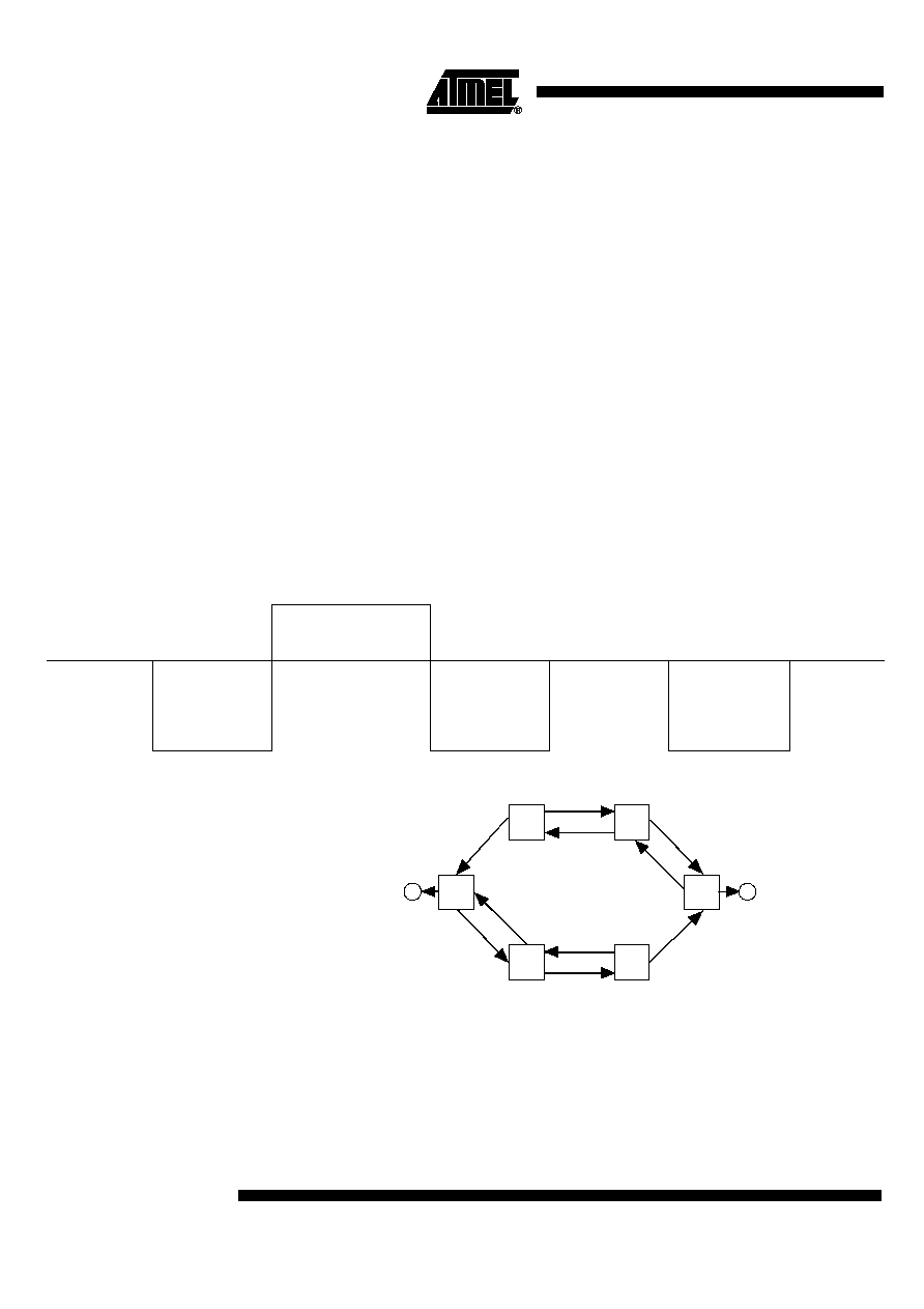
Figure 4. Watchdog Timing Diagram with Tolerances
Figure 5. Watchdog State Diagram
Explanation
In each block, the first character represents the state of the counter. The second nota-
tion indicates the fault status of the counter. A fault status is indicated by an "F" and a
no-fault status is indicated by an "NF". When the watchdog is powered up initially, the
counter starts at the 0/F block (initial state). "Good" indicates that a pulse has been
received whose width resides within the timing window. "Bad" indicates that a pulse has
been received whose width is either too short or too long.
Time/s
79/ f
WDC
80/ f
WDC
169/ f
WDC
170/ f
WDC
250/ f
WDC
251/ f
WDC
Watchdog Window
update rate is good
Update rate is
too fast
Update rate is
either too fast or
good
Update rate is
either too slow
or good
Update rate is
too slow
Update rate is
either too slow
or pulse has
dropped out
Pulse has
dropped out
1/NF
2/NF
O/F
1/F
2/F
3/NF
bad
good
bad
good
bad
good
good
bad
good
good
bad
bad
Initial status

5
U6813B
4543A≠AUTO≠05/02
Watchdog Window
Calculation
Example with recommended values
C
osc
= 6.8 nF (should be preferably 10%, NPO)
R
osc
= 36 k
W
(can be 5%, R
osc
< 200 k
W
due to leakage current and humidity)
RC oscillator
t
WDC
(s) = 10
-3
[C
osc
(nF) [(0.00078 R
osc
(k
W
)) + 0.0005]]
f
WDC
(Hz) = 1 / (t
WDC
)
Watchdog WDI
f
WDI
(Hz) = 0.01 f
WDC
t
WDC
= 200 µs
Æ
f
WDC
= 5 kHz
f
WDI
= 50 Hz
Æ
t
WDI
= 20 ms
WDI pulse width for fault detection after 3 pulses:
Upper watchdog window
Minimum: 169/ f
WDC
= 33.8 ms -> f
WDC
/ 169 = 29.55 Hz
Maximum: 170/ f
WDC
= 34 ms -> f
WDC
/ 170 = 29.4 Hz
Lower watchdog window
Minimum: 79/ f
WDC
= 15.8 ms -> f
WDC
/ 79 = 63.3 Hz
Maximum: 80/ f
WDC
= 16 ms -> f
WDC
/ 80 = 62.5 Hz
WDI dropouts for immediate fault detection:
Minimum: 250/ f
WDC
= 50.0 ms
Maximum: 251/ f
WDC
= 50.2 ms
Remarks to reset relay
The duration of the over- or undervoltage pulses determines the enable- and reset out-
puts. A pulse duration shorter than the debounce time has no effect on the outputs. A
pulse longer than the debounce time results in the first reset delay. If a pulse appears
during this delay, a second delay time is triggered. Therefore, the total reset delay time
can be longer than specified in the data sheet.