 | –≠–ª–µ–∫—Ç—Ä–æ–Ω–Ω—ã–π –∫–æ–º–ø–æ–Ω–µ–Ω—Ç: U6820BM | –°–∫–∞—á–∞—Ç—å:  PDF PDF  ZIP ZIP |
1
Features
∑
Four Short-circuit-protected High-side Drivers with a Maximum Current Capability of
50 mA Each
∑
Four Short-circuit-protected Low-side Drivers with a Maximum Current Capability of
50 mA Each
∑
ON Resistance High Side R
on
< 10
Versus Total Temperature Range
∑
ON Resistance Low Side R
on
< 7
Versus Total Temperature Range
∑
Short-circuit Detection of Each Driver Stage
∑
Disabling of Driver Stages in the Case of Short-circuit and Overtemperature Detection
∑
Independent Control of Each Driver Stage via an 8-bit Shift Register
∑
Status Output Reports Short-circuit Condition
∑
Status Output Reports when All Loads Are Switched Off
∑
Timing of Status Output Reset Signalizes Failure Mode
∑
Temperature Protection in Conjunction with Short-circuit Detection
Description
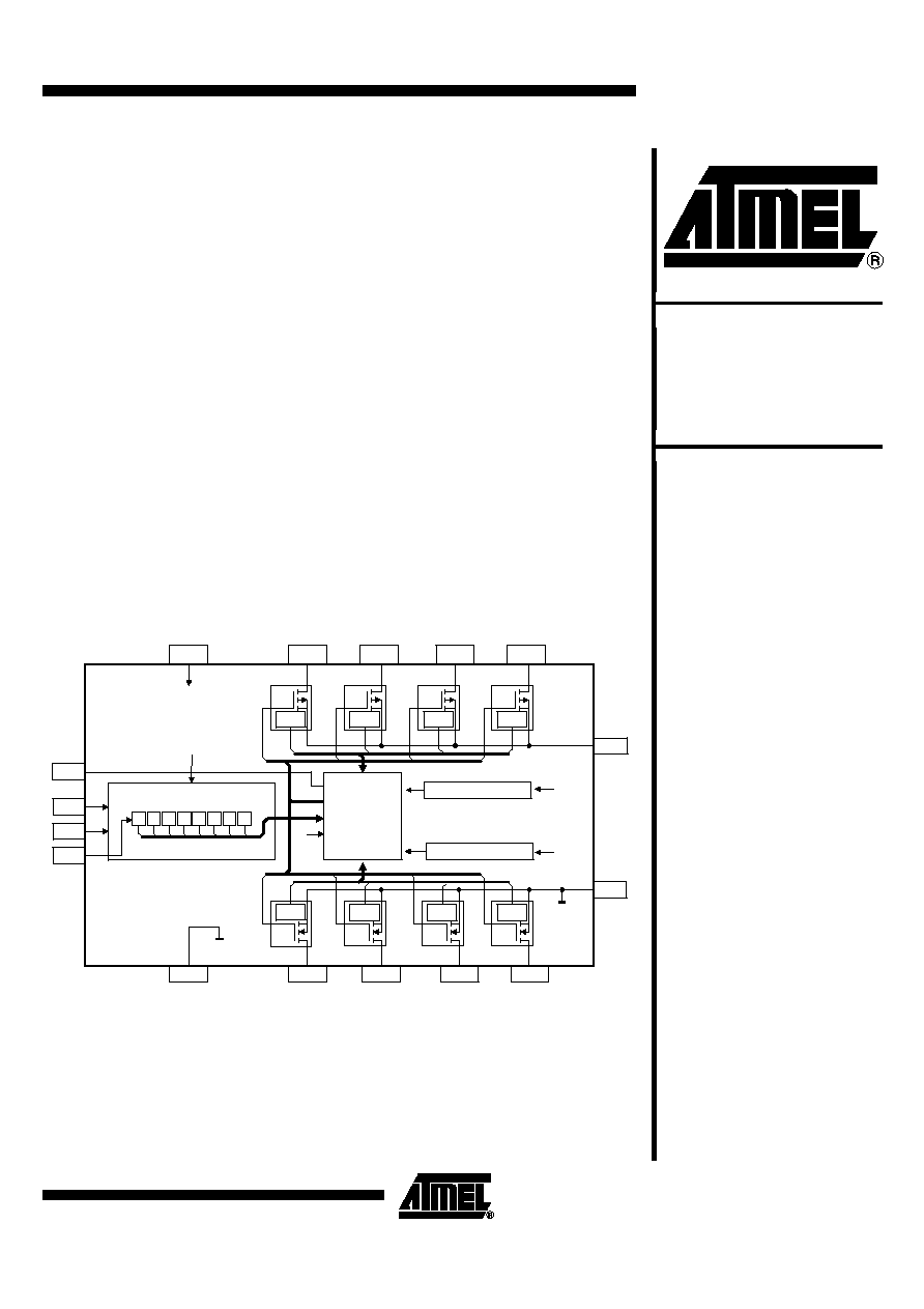
The U6820BM is a driver interface in BCDMOS technology with 8 independent driver
stages having a maximum current capability of 50 mA each. Its partitioning into 4
high-side and 4 low-side driver stages allows an easy connection of either 4 half-
bridges or 2 H-bridges on the pc board. The U6820BM communicates with a micro-
controller via an 8-bit serial interface. Integrated protection against short circuit and
overtemperature give added value. EMI protection and 2-kV ESD protection together
with automotive qualification referring to conducted interference (ISO/TR 7637/1)
make this IC ideal for both automotive and industrial applications.
Figure 1. Block Diagram
V
CC
STATUS
CLK
DI
CS
HS4
HS3
HS2
HS1
Thermal protection
6
9
8
1
Control
logic
16
3
Power-on reset
V
CC
V
CC
2
7
10
15
5
V
CC
V
CC
4
14
11
13
12
LS1
LS2
LS3
LS4
GND
CC
H
H
3
S
S
4
S
2
S
1
L
S
3
L
S
4
L
S
2
L
S
1
Input Register
H
H
Current
limiter
Current
limiter
Current
limiter
Current
limiter
Current
limiter
Current
limiter
Current
limiter
Current
limiter
GND S
V
S
Dual Quad
BCDMOS
Driver IC
U6820BM
Rev. 4527A≠BCD≠03/02

2
U6820BM
4527A≠BCD≠03/02
Pin Configuration
Figure 2. Pinning SO16
1
2
3
4
5
6
7
8
16
15
14
13
12
11
10
9
VS
GNDCC
GNDS
VCC
LS2
HS2
HS1
LS1
STATUS
DI
CLK
CS
LS3
HS3
HS4
LS4
Pin Description
Pin
Symbol
Function
1
HS1
Output high side 1
2
LS1
Output low side 1
3
VS
Supply voltage 6 V to 18 V
4
GNDCC
Digital ground
5
GNDS
Power ground
6
VCC
Supply voltage 5 V (external)
7
LS2
Output low side 2
8
HS2
Output high side 2
9
HS3
Output high side 3
10
LS3
Output low side 3
11
CS
Set supply status (chip select)
12
CLK
Clock line for 8-bit control shift register
13
DI
Data line for 8-bit control shift register
14
STATUS
Status output (H = fault, diagnostic "H" if all driver stages are switched off)
15
LS4
Output low side 4
16
HS4
Output high side 4

3
U6820BM
4527A≠BCD≠03/02
Description of the
Control Interface to
the Microcontroller
The serial-parallel interface basically includes an 8-bit shift register (SR), an 8-bit com-
mand register (CR) and a 4-bit counter.
The data input takes place with commands at Pins DI (data input), CS (chip select) and
CLK (clock). With a falling edge at CLK, the information at DI is transferred into the SR.
The first information written into the SR is the least significant bit (LSB). The Pin STA-
TUS is used for diagnostic purposes and reports any fault condition to the
microcontroller.
The input CS in accordance with the CR controls the serial interface. A high level at CS
disables the SR. With a falling edge at CS, the SR is enabled. The CR control allows
only the first 8 bits to be transferred into the SR, and further clocks at CLK are ineffec-
tive. If a rising edge occurs at CS after 8 clocks precisely, the information from the SR is
transferred into the CR. If the number of clock cycles during the low phase of CS was
less or more than eight transitions, no transfer will take place. A new command switches
the output stages on or off immediately.
Each output stage is controlled by one specific bit of the CR. Low level means "supply
off" or inactive, and high level means "supply on" or active. If all 8 bits are at a low level,
the output stages will be set into standby mode.
If one of the output stages detects a short circuit and additionally overtemperature con-
dition, the corresponding control bit in the CR is set to low. This reset has priority over
an external command to CR, thus, this does not affect the 1
st
control bit. The priority pro-
tects the IC against overtemperature by activating the temperature shut down
immediately.
The STATUS Output
The STATUS output is at low level during normal operation. If one or more output stages
detect short circuit or if overtemperature is indicated, the STATUS output changes to
high level (OR-connection).
For diagnostic purposes (self test of the status output), the status output can also be
brought into high level during standby mode.
Timing of the Status
Output Reset Signalizes
the Failure Mode
The use of different reset conditions at the STATUS output simplifies the failure analysis
during normal operation, and is also beneficial during testing.
The storage content can be used for STATUS output. It is indicated and latched immedi-
ately with the rising edge of CS at STATUS output if less than 8 clocks were received
during the low phase of CS. The reset is initiated by the falling edge of the 8
th
clock
(bit 7) of the next data input.
Also, the appearance of more than 8 clocks is latched and indicated at STATUS by the
rising edge of the 9
th
clock. The reset is initiated by the falling edge of the 2
nd
clock
(bit 1) of the next data input.
The detection of overtemperature is latched internally. It is reset by the falling edge of
the 4
th
clock (bit 3) of a data transfer if overtemperature is no longer present.
Power-on Reset
After switching on the supply voltage, all data latches are reset and the outputs are
switched off. The typical power-on reset threshold is V
CC
= 3.7 V. The outputs are acti-
vated after the first data transfer.
4
U6820BM
4527A≠BCD≠03/02
Short-circuit Protection
The current of the output stages is limited by an active feedback control. Short circuit at
one output stage sets the diagnostic Pin 14 (STATUS) to high. In case of both condi-
tions, short circuit at one of the outputs and temperature detection, the affected output is
switched off selectively. It will be activated again after the first new data transfer.
Inductance Protection
Clamping diodes and FETs are integrated to protect the IC against too high or too low
voltages at the outputs. They prevent the IC from latch up and parasitic currents which
may exceed power dissipation.
Temperature Protection
The IC is protected by an overtemperature detection. As soon as the junction tempera-
ture T
j
= 155
∞
C typically is exceeded, the diagnostic Pin 14 (STATUS) is set "high".
General overtemperature detection along with short-circuit condition at a specific output
result in temperature shut down at that specific output. After temperature shut down, the
data input register has to be set again with a hysteresis of typically
T = 15 K
(T
j
= 140
∞
C).
ESD Protection
All output stages are protected against electrostatic discharge up to 5 kV (HBM) with
external components (see Figure 5), all other pins are protected up to 2 kV (HBM).
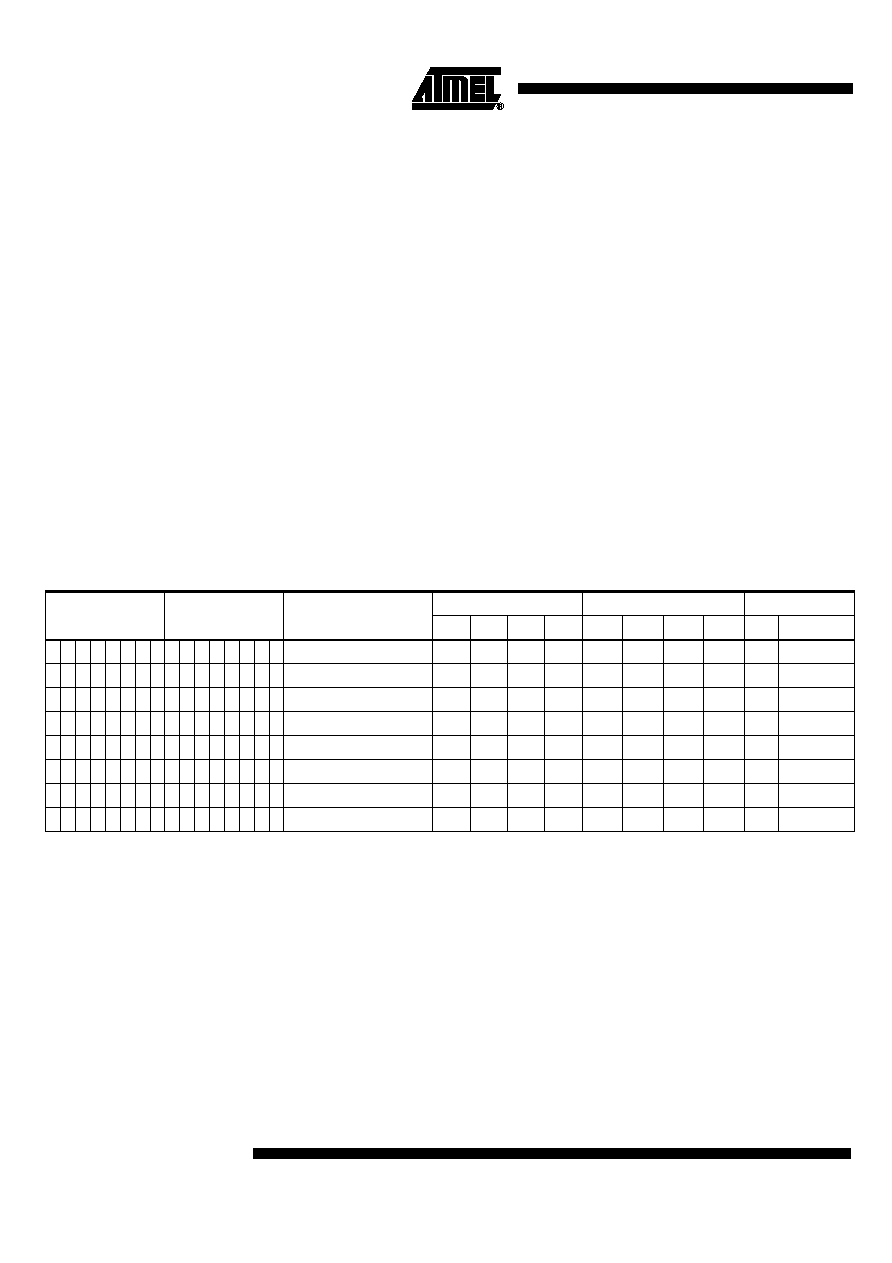
Table 1. Timing of the STATUS Output
Shift Register
Command
Register
Condition
Low-side Switch
High-side Switch
Status
LS1
LS2
LS3
LS4
HS1
HS2
HS3
HS4
Set
Reset
0 0 0 0 0 0 0 0 0 0 0 0 0 0 0 0
All out = OK
off
off
off
off
off
off
off
off
H
New CS
1 1 1 1 1 1 1 1 1 1 1 1 1 1 1 1
All on = OK
on
on
on
on
on
on
on
on
L
0 0 0 0 0 0 0 1 0 0 0 0 0 0 0 1
E.g. one on = OK
off
off
off
off
off
off
off
on
L
0 1 1 1 1 1 1 1 0 1 1 1 1 1 1 1
Short at LS3
off
on
on
on
on
on
on
on
H
No short
1 1 1 1 1 1 1 1 1 1 1 0 1 1 1 1
Temp & short at HS4
on
on
on
off
on
on
on
on
H
New CS4
1 1 0 0 0 0 1 1 0 0 0 0 0 0 0 0
V
VCC
< 3.7 V = P-ON
off
off
off
off
off
off
off
off
H
P-ON, CS
1 1 1 0 0 0 1 1 x x x x x x x x
CS with less 8 CLK
x
x
x
x
x
x
x
x
H
New CS 8
0 0 0 1 1 1 0 0 x x x x x x x x
CS with more 8 CLK
x
x
x
x
x
x
x
x
H
New CS 2
5
U6820BM
4527A≠BCD≠03/02
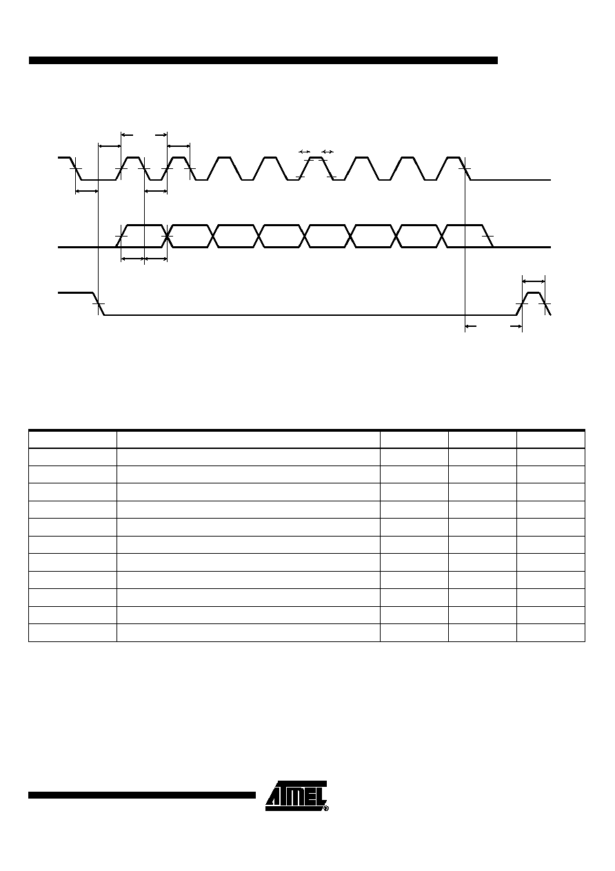
Figure 3. Data Transfer Timing Diagram
Table 2. AC Characteristics for Testing
Specification
Conditions
Minimum
Maximum
Unit
t
r
(rise)
10% to 90% V
CC
on CLK, DI and CS
10
ns
t
f
(fall)
10% to 90% V
CC
on CLK, DI and CS
10
ns
t
CLKP
1/2 V
CC
250
ns
t
CLKH
1/2 V
CC
100
ns
t
CLKL
1/2 V
CC
100
ns
t
CLKCS
1/2 V
CC
150
ns
t
CSCLK
1/2 V
CC
100
ns
t
DICLK
1/2 V
CC
80
ns
t
DIH/L
1/2 V
CC
100
ns
t
CLKCSH
1/2 V
CC
100
ns
t
CS
1/2 V
CC
250
ns
t
CSCLK
t
CLKP
t
CLKH
t
CLKL
t
DICLK
t
DIH/L
t
CLKCS
50%
50%
50%
t
CLKCSH
t CS
CLK
DI
CS
90 %
10%
t
r
90 %
t
f
LSB
MSB