 | Электронный компонент: UG1 | Скачать:  PDF PDF  ZIP ZIP |

FPGA Design
6¡1
Rev. B
¡
25 May. 98
Scope
This Application Note describes design practices that
make a ULC conversion schedule shorter, and accom-
plished with reduced risk. This note is recommended for
a designer considering a conversion to a ULC, or for a de-
signer before starting an FPGA design. For the designer
considering a conversion to a ULC, this Application Note
will give background on the reasons for the questions in
the ULC Design Checklist. For the designer just starting
and FPGA design, this Application Note shows that much
can be done during the FPGA design process to reduce the
ULC conversion schedule and risk. This application note
is probably not needed by an experienced ASIC designer,
because the experienced ASIC designer is almost certain-
ly following these design practices already.
This Application note is in three sections:
D Overcoming Timing Difficulties ¡ An Introduction to
Good Design Practices
D Good Design Practices.
D Good Simulation Practices.
These "good design practices" also apply to good FPGA
design, even if not converting to a ULC, and to good ASIC
design.
Although following these practices is not mandatory, it is
recommended. In all cases, for a ULC conversion, a feasi-
bility study is done first to determine if a conversion
should be successful. The feasibility study includes a de-
termination of the degree of conformance to these practic-
es, and an assessment of the degree of difficulty of a con-
version. If these good design practices have been
followed, it is virtually assured that the results of the feasi-
bility study will be positive; if the practices have not been
followed, there is a chance that the results of the feasibil-
ity study will be negative.
Note that the effective use of CAD/CAE tools depends on
the designer following these design practices. If good de-
sign practices have been followed, the tools work much
better, faster, with much less manual intervention, and re-
port fewer errors and warnings that must be resolved by
the ULC designer.
Overcoming Timing Difficulties ¡ An
Introduction to Good Design Practices
First a word about good FPGA design practices. Good
FPGA design practices include allowing margins for tim-
ing variations. Timing variations occur as the chip oper-
ates over a temperature range, and due to fabrication pro-
cess variations. When a designer uses trial and error in the
system lab to design an FPGA, with no system¡level
specification for the FPGA and little knowledge of timing
margins, the resulting FPGA could be undependable over
temperature and process. FPGA designers should use
good design practices, and simulation, to make sure that
this does not happen. However, note that if the FPGA op-
erates in production without problems for some time, this
is proof that it is likely that adequate timing margins exist.
Now, on to conversion considerations. Converting the
FPGA design to anything else (not just ULCs) means re¡
targeting the design to a new set of timing parameters,
similar to those of the FPGA, but not exactly the same.
A ULC is smaller and generally faster, like most ASICs,
relative to an FPGA. The fastness of the ULC can be a
problem if the FPGA requires long delays on some paths.
On the other hand, the ULC can be slower than Global
Clock (fast¡path) features on FPGAs, and this can be a
problem if the signal travels across the chip. Also, ULC
setup and hold are usually different; ULC setup is about
zero, and hold is about 2¡5ns, whereas FPGA setup and
hold is generally the opposite. ULC designers know how
to handle the conversions, but the conversion is much eas-
ier if the FPGA designer uses good design practices, and
simulation.
If the timing tolerances are known, Atmel Wireless & Mi-
crocontrollers assures that a successful FPGA conversion
can be achieved, whether or not the FPGA has been simu-
lated. This is assured by using ATPG (Automatic Test
Program Generation) and associated fault simulation/
grading. Before tapeout of the ULC, the ULC vectors,
whether generated by the customers' simulations or by
Atmel Wireless & Microcontrollers ATPG, are tested on
the FPGA in an IC tester, where timing is analyzed, and
functionality is verified if tester or simulation vectors are
provided by the customer.
Note that only customer¡provided vectors will check for
correct functional operation; the Atmel Wireless & Mi-
crocontrollers ATPG vectors are used to check logic con-
formance to a customer specification and/or within toler-
ance of the FPGA timing, but these latter vectors do not
check functionality (so the logic in the FPGA had better
represent the desired functionality). Also note that only
pin¡to¡pin vectors contribute to assuring the correctness
Good FPGA Design Practices, Aid FPGA Conversion to a
ULC

FPGA Design
6¡2
Rev. B
¡
25 May. 98
of the conversion; simulation vectors that set internal
nodes during simulation are welcome information but do
not directly aid in checking the conversion. Also, note the
Test Vectors, used after fabrication, are created from cus-
tomer¡provided vectors and may not reach 85% of fault
coverage as required. In this case, Atmel Wireless & Mi-
crocontrollers inserts scan to increase fault coverage. Of
course, JTAG is supported.
Atmel Wireless & Microcontrollers has proven tech-
niques that have been used to convert hundreds of
FPGAs, many done when the original FPGA designer
was not available to answer questions. However, we al-
ways do a (free) feasibility study to make sure that the
conversion should succeed, and the result of the feasibil-
ity study is generally positive.
Good Design Practices
Atmel Wireless & Microcontrollers ULC designers use a
"Feasibility Risk Assessment" checklist to record their
analysis of the FPGA submitted for a feasibility study.
This checklist covers the design practices described in
this Application Note, and it makes sure that the ULC de-
signer assesses the potential problems in those areas
where good design practices have not been followed and
therefore there is increased risk that the conversion will
take longer, or be unsuccessful, unless appropriate mea-
sures are taken. This sheet is shown in Figure 1. The fol-
lowing paragraphs are a description of these items, in the
same order, and same numbering, as the table.

FPGA Design
6¡3
Rev. B
¡
25 May. 98
Figure 1. Feasibility Risk Assessment (Rev. 1)
Mask & Company Name:
Date:
Feasibility Study Designer(s):
j With Vectors
j Without Vectors
ANALYZE THE FOLLOWING
(Assign a risk factor if the "good design
practice" has not been used)
Risk Rating
(0¡10; 10 is bad)*
Estimated Extra Days if
Need
COMMENTS:
1. Timing Well¡specified (internal and
external), i.e., a specification (with timing)
2. Master Clear (Initialization); or small set of
vectors to get to known state; a way to
circumvent POR (if any)
3. Only FFs drive reset (No combinatorial
logic driving reset)
4. Avoided Gated Clocks
5. Avoided internally¡generated clocks (used
on¡chip)
6. Avoided Counters or control states over 10
bits without taps
7. Glitches into a FF data¡in before clk
8. Avoided combinatorial loops (including no
home¡made FFs)
9. Avoided internal tri¡states
10.Avoided redundant or fault tolerant circuits
11.Avoided Global Clocks too fast to meet tim-
ing; & delay blocks or programmed delays; &
deglitching circuits
12.Avoided demand for high fault coverage,
e.g., 95%
13.Avoided special noise standards
14.Avoided Asynchronous circuits
15.No dynamic programming (fatal)
TOTALS:
1. Write a specification on functionality and timing of the
FPGA. This is for the reasons described above. Also,
provide schematics and other items listed on the Custom-
er questionnaire.
2. Use Master Clear, i.e., an asynchronous reset from an
external pin. Second best is a small set of vectors to get
to a known state. This means that there must be a way to
circumvent any POR (Power On Reset), and rapidly get
to a known state. Timing cannot be verified using simula-
tion if the logic cannot be efficiently taken to a known
state. The same is true for fault simulation/grading (used
to generate tests that determine if the fabrication process
is OK, and if enough logic has been tested to assure a suc-
cessful conversion ). (Don't use a bi¡direct buffer on re-
set, or clock inputs, because it will make a mess of the
simulation vectors when it goes to the Z state.)
3. Use only FFs to drive Reset (in addition to master
Clear). In other words, the reset to a FF needs to be syn-
chronized and stabilized, and this is done by driving the
reset from a data output of another FF, or else glitches can
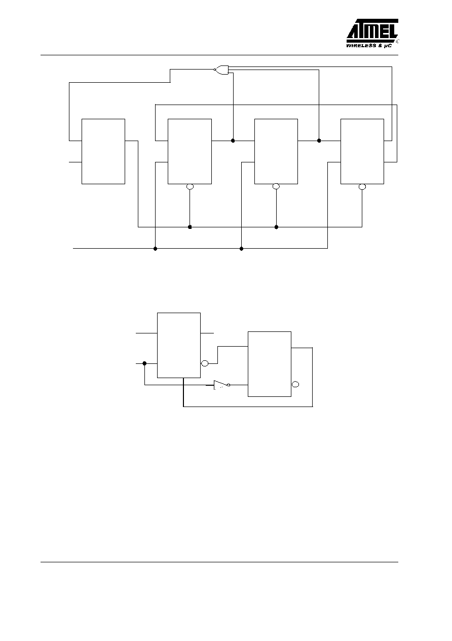
occur, causing errors. So, for example, the correct
construction of a divide¡by¡3 counter would be as shown
in Figure 2.
FPGA Design
6¡4
Rev. B
¡
25 May. 98
D
Q
NQ
D
Q
CK
NQ
D
Q
CK
NQ
D
Q
CK
NQ
NCK
CK
NR
NR
NR
CK
Figure 2. Correct Construction of a Divide¡by¡3 Counter
Also, if you need to generate a short pulse, instead of connecting a FF's Q to its reset, do as shown in figure 3.
D
Q
NQ
D
Q
CK
NQ
CK
CK
IN
OUT
R
Figure 3. If Must Make Pulses, Do It This Way
4. Try to minimize the use of gated clocks, because they
cause more skew between the clock and the data. In lay-
out, the skew can be a real challenge to accommodate. If
the skew cannot be accommodated, spikes occur. Of
course, an enable on the clock that has been built into the
cell library is OK, because this circuit is specially con-
trolled by the CAE tools, including the layout tools, but
designer¡generated gated clocks cause errors and warn-
ings by the CAE tools and, if there are enough of them
spread around the logic, layout may not be able to get rid
of the skew everywhere, and the conversion may have to
be aborted (aborted toward the end of the design phase,
which means that much design time will have been
wasted).
5. Try to minimize internally generated and used clocks
(created using sequential or combinatorial logic), because
the distribution of such clock lines inside the chip are sub-
ject to skew that may not be accounted for by clock tree
generation software and thus will likely have skew prob-
lems. This is similar to the problems in items 3 and 4. (So
use of equations to generate clock signals in an FPGA de-
sign is not advised.)
6. Try to keep counters, dividers, control state logic, etc.,
segments to less than 10 bits, as seen from the input/out-
put pins, or add taps. If more than 10 bits, long counters
should have taps for monitoring, or at least have a pre¡
load function. These taps should somehow easily propa-

FPGA Design
6¡5
Rev. B
¡
25 May. 98
gate their data to output pins. The reason for this good
practice is that the number of simulation vectors and test
times required are too much without it.
7. Construct logic to minimize glitches, and when a glitch
is unavoidable, make sure that it settles out at the data in-
put of a FF (Flip Flop) before this FF is clocked. Also,
glitches into reset, set, or clock inputs to a flip flop must
be avoided; as stated above, we recommend not using
combinatorial logic in reset, set, or clock in the first place.
8. Avoid combinatorial loops (including combinatorial
latches), and pulse generators. Any combinatorial design
whose proper operation depends on delays through logic
elements is dangerous. This is especially true in ULCs
and ASICs but is also true for FPGAs. So don't design as-
suming that the delay down any combinatorial path is pre-
dictable, and that the difference in time down two differ-
ent paths to the same destination is predictable. It isn't
(unless very carefully controlled, as is done when creating
the logic inside the cell of a cell library). Pulse widths and
delays vary substantially over temperature, process varia-
tions, re¡layouts, and voltage variations.
9. Internal tri¡states are best avoided, although we prob-
ably can handle them with some difficulty. If internal tri¡
states are unavoidable, avoid floating nodes. These can
occur when all of the buffers driving a bus are disabled.
Add a buffer to drive the bus when all of the other buffers
are OFF.
10. Try to avoid redundant or fault tolerant circuits, al-
though we can handle them with some difficulty. The dif-
ficulty comes during re¡synthesis to the ULC, where re-
dundant logic is minimized out (and thus must be
manually added back in). Please inform us if this type of
circuitry is in your design.
11. Minimize the use of global clocks (fast paths), delay
blocks, programmed delays, and deglitching circuits, be-
cause it is difficult (but generally not impossible) to match
the timing. The Global Clock is only a problem when
converting (to a ULC) if the signal travels across the chip.
The delay blocks and programmed delays are problems
because any function that depends on delay of the logic
elements is difficult to reproduce (the min/max delay
window in the converted material is too big), as explained
in item 8 above. Deglitching circuits are also difficult to
reproduce for the same reason ¡ the min/max delay win-
dow in the converted material is too big.
12. Try not to insist on high fault coverage (e.g., 95%).
Although it sounds good to demand the same fault cover-
age as on an ASIC, this adds to the time (and thus cost) of
the conversion and does not provide the degree of benefit
it does for an ASIC. First of all, ASICs are designed with
design¡for¡test rules so that scan logic can be efficiently
added, and its supporting CAE tools will work efficiently.
FPGAs usually are not designed using these rules. The
good design practices of this Application Note are nearly
the same as the design¡for¡test rules for scan, so if these
good design practices are followed completely, adding
scan should not be a problem. However, if the practices
are not rigorously followed, adding scan can take much
time, and, in a few cases, may not be made to work proper-
ly. (Scan is a method where logic is added to each flip flop
to allow all of the flip flops to be connected in a serial
string in test mode so that test bits can be inserted and ex-
tracted in/out of the FFs between each normal clock pulse,
effectively turning the flip flops into I/O pins for test, thus
eliminating the very negative effect of the flip flops on
generating an effective test using just real I/O pins.) We
try to achieve 85% fault coverage without adding scan.
Keep in mind that the merit of high fault coverage is that
it provides a somewhat better check on the fabrication
process ¡ it contributes nothing to the accuracy of the con-
version. We have other ways to check the fabrication pro-
cess, including conservative process and packaging yield
monitoring, and IDDQ testing can be added if the custom-
er deems it necessary. Of course all of this will not be an
issue if the fault coverage percentage gets to 95% without
adding scan logic, as is often the case. On the other hand,
at the other extreme, if the design has a big function but
few pins in and/or out, e.g., a digital filter, we may not be
able to achieve a great enough fault coverage percentage
to be confident of the conversion, not to mention the mon-
itoring of the processing. In other words, our primary
concern is an accurate conversion, which depends on get-
ting the fault coverage up using testing from the I/O pins
only, and adding scan logic will not help this (at least at
present¡day levels of relatively low logic usage in FPGAs
as converted). We have found that 85% test coverage is
good; 60% is OK; and under 50% is definitely risky.
13. Let us know about any noise requirements or stan-
dards that must be met, because we can use our slow slew
rate buffers to avoid noise problems (we have slew rate
control).
14. Try to use synchronous design as much as possible,
because asynchronous design often depends on element
delays, which, as we said in several places above, is diffi-
cult to duplicate in a conversion.
15. No dynamic reprogramming if you plan to do a con-
version. We can handle on¡board RAM, but not if used
for dynamic re¡programming. In other words, we can
generally assure timing with one set of program parame-
ters in an FPGA but it gets too complicated when these pa-
rameters are changed on the fly. So, in fact, we only hard¡
wire the programmed parts. (Note that this means that, for
FPGAs that use the daisy chain method of programming,
we can convert all of this set of FPGAs, or any FPGAs
that are not the master, but we can't be the master when
the slaves are not our conversions, i.e., not if the slaves are
expecting to be programmed. That is, our converted
slaves simply pass the programming data down the daisy
chain. Our master cannot generate daisy chain program-
ming information.)