
KSD-I6O001-000
1
S1117AD/S1117-xxD
Adjustable and Fixed Voltage Regulator
Descriptions
The S1117 series of positive adjustable and fixed regulators are designed to provide 1A with high efficiency.
All internal circuitry is designed to operate down to 1.3V input to output differential. On-chip trimming adjusts
reference voltage to 2%.
Features
∑ Adjustable or fixed output
∑ Output current of 1A
∑ Low dropout, 1.3V maximum at 1A output current
∑ Thermal shutdown protection
Ordering Information
Type NO.
Marking
Package Code
S1117AD/S1117xxD S1117D/ S1117
D D-PAK
:Voltage Code (Aj : 1.25V, 15:1.5V,:18: 1.8V, 25:2.5V, 33:3.3V, 50:5.0V)
:Voltage Code (285:2.85V)
Outline Dimensions
(Unit : mm)
S
S
e
e
m
m
i
i
c
c
o
o
n
n
d
d
u
u
c
c
t
t
o
o
r
r
PIN Connections
1. GND / Adj.
2,4 Output
3. Input
BLOCK DIAGRAM

KSD-I6O001-000
2
S1117AD/S1117-xxD
Absolute Maximum Ratings
[Ta=25
∞C]
Characteristic Symbol
Rating
Unit
Input voltage
V
I
16
V
P
D
1(Note1) 4.5
Power Dissipation
P
D
2(Note2) 1.5
W
Junction Temperature
T
J
150
∞C
Operating temperature range
T
opr
0 ~ +125
Storage temperature range
T
stg
-55 ~ +150
∞C
Note 1 : Mounted on a glass epoxy circuit board of 50.8 ◊ 50.8mm. (at 1oz copper area)
Note 2 : No Heat sink
Recommended operating conditions
Characteristic Symbol
Min.
Max.
Unit
Input voltage
V
I
V
O
+1.5V V
O
+7V V
Output current
I
O
1
1000
mA
Device Selection Guide
Note 3 : Other fixed versions are available V
O
=1.5V ~ 5V
Device Output
Voltage
S1117AD Adjustable
S1117-15D 1.50V
S1117-18D 1.80V
S1117-25D 2.50V
S1117-285D 2.85V
S1117-33D 3.30V
S1117-50D 5.00V
KSD-I6O001-000
3
S1117AD/S1117-xxD
Electrical Characteristics
(Electrical Characteristics at 0T
a
125 and V
I
=(V
O
+1.5V), Io=10mA, C
O
=10µF, unless otherwise specified.)
Characteristic Symbol Device
Test Condition
Min Typ Max
Unit
*
1.23
1.28
S1117A
V
I
= (V
O
+1.5V) to 7V
I
O
= 0 to 1000mA
1.20
1.25
1.30
*
1.47
1.53
S1117-15
V
I
= (V
O
+1.5V) to 7V
I
O
= 0 to 1000mA
1.44
1.50
1.56
*
1.76
1.84
S1117-18
V
I
= (V
O
+1.5V) to 7V
I
O
= 0 to 1000mA
1.73
1.80
1.87
*
2.45
2.55
S1117-25
V
I
= (V
O
+1.5V) to 7V
I
O
= 0 to 1000mA
2.40
2.50
2.60
*
2.79
2.91
S1117-285
V
I
= (V
O
+1.5V) to 7V
I
O
= 0 to 1000mA
2.74
2.85
2.96
*
3.23 3.30 3.37
S1117-33
V
I
= (V
O
+1.5V) to 7V
I
O
= 0 to 1000mA
3.17 3.43
*
4.90 5.00 5.10
Output voltage
V
O
S1117-50
V
I
= (V
O
+1.5V) to 7V
I
O
= 0 to 1000mA
4.80 5.20
V
Line regulation
(Note4)
V
O(VI)
All
1.5V V
I
-V
O
7V
I
O
=10mA
*
- 5 10
mV
Load regulation
(Note4)
V
O(IL)
All
1.5V V
I
-V
O
7V
I
O
=10mA ~ 1000mA
*
- 10 30 mV
Quiescent
current
I
QC
All
I
O
=0 -
7
13
mA
Minimum load
current
I
L(MIN)
S1117A
V
Adj
=0V
3
7
mA
Adjust pin
current
I
ADJ
S1117A
V
I
= (V
O
+1.5V) to 7V
I
O
= 100mA
55 90
µA
Adjust pin
current change
I
ADJ
S1117A
1.5V V
I
-
V
O
7V
I
O
=10mA ~ 1000mA
1 5
µA
Dropout voltage
V
DROP
All
I
O
=1000mA
*
-
1.2
1.3
V
Ripple rejection
ratio
RR All
I
O
=1000mA
V
Ripple
=1V
P-P
, f=120
*
60 72
-
dB
Current limit
I
LIMIT
All
I
O
1000mA
*
1.1
A
[ * ] Ta=25
Note 4: Low duty pulse testing with Kelvin connections required.
KSD-I6O001-000
4
S1117AD/S1117-xxD
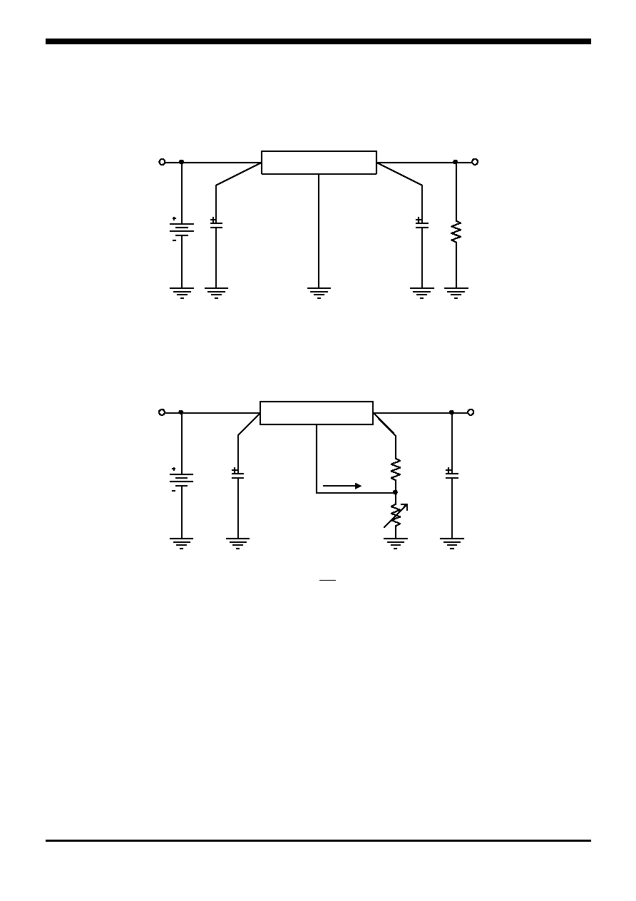
Typical Applications
Fig. 1 Fixed Voltage Regulator
2
ADJ
1
2
ADJ
R
◊
I
+
)
R
R
+
1
(
◊
V
=
Vo
Fig. 2 Adjustable Voltage Regulator
V
S1117A
10
C
(Adjustable Version)
R
I
R
I
125
(1
)
O
225
(1
)
O
C
10
1
V
Vo=3.5V
2
Adj
Notes 5:
1) C
I
needed if device is far from filter capacitors
2) C
O
minimum value required for stability
I
ADJ
R
10
O
10
O
S1117-XX
V
V
(Fixed Version)
L
Adj/GND
I
C
C
I
KSD-I6O001-000
5
S1117AD/S1117-xxD
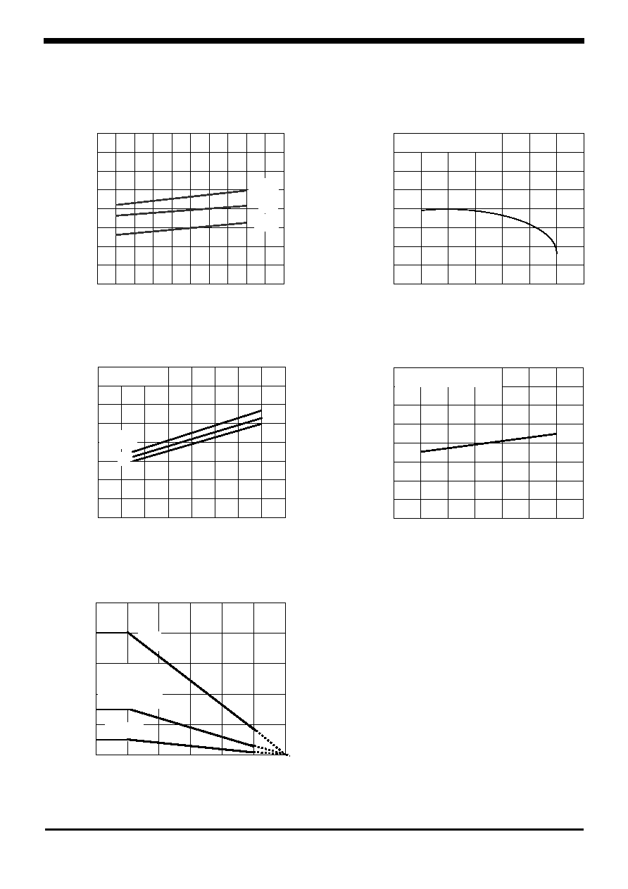
Electrical Characteristic Curves
Fig.3 V
DROP
vs I
O
Fig.4 Vo
vs T
a
1.8
200
1000
600
400
1.4
0
800
2.0
0.8
0.4
0.6
1.6
1.2
1.0
Dro
pou
t Vo
ltag
e
V
DROP
[V
]
Output Current I
O
[mA]
Ta=0∞C
50∞C
125∞C
Out
put
V
o
l
t
a
g
e
De
vi
at
i
on [%
]
Ambient Temperature T
a
[]
0
150
75
50
-25
100
25
125
0.90
0.30
1.20
-0.6
-1.2
-0.9
0.60
0.00
-0.3
V
I
=V
O
+1.5V, I
O
=500mA
Fig.5 I
L(MIN)
vs V
I
-V
O
Fig.6 I
Adj
vs Ta
Input-Output Differential Voltage [V]
1.0
8
1.8
3.4
2.6
0
6
3
4.2
M
i
n
i
mu
m L
o
ad
Cu
rr
en
t
I
L(MIN)
[m
A]
4
1
2
5
7
1.4
2.2
3.0
3.8
Ta=125
50
0
Fig.7 P
D
vs T
a
Ambient Temperature T
a
[∞C]
100
50
15
25
9
125
75
150
12
3
6
0
0
Po
wer di
ssi
pat
i
o
n
P
D
[W
]
Adj
u
st Pi
n Cu
r
r
ent
I
Adj
[µ
A]
Ambient Temperature T
a
[]
0
150
75
50
-25
100
25
125
T
C
=25∞C
Ta=25
Mounted on a glass
epoxy circuit board
of 50.8*50.8 mm
(at 1oz copper area)
80
70
85
55
40
45
75
65
60
V
I
=V
O
+1.5V, I
O
=100mA
S1117A, V
Adj
=0