
KSI-L011-000
1
S4560P
Dual high slew rate OP AMP
F
Description
The S4560P is dual operational amplifiers which achieve approximately twice the high
output current of the S4560P, as well as featuring a higher slew rate of 4V/us, a gain band
width of 10MHz, and an improved frequency characteristic.
Features
∑ Built-in output short-circuit protection circuit.
∑ Internal phase correction.
∑ No latch-up
∑ Wide same phase mode and differential voltage ranges
∑ High gain. low noise
Applications
∑ Active filters
∑ Audio amplifiers
∑ VCOs
∑ Other electronic circuits
Ordering
Information
Type NO. Marking Package Code
S4560P S4560P DIP-8
Outline Dimensions unit :
mm
S
S
e
e
m
m
i
i
c
c
o
o
n
n
d
d
u
u
c
c
t
t
o
o
r
r
Block Diagram
KSI-L011-000
2
S4560P
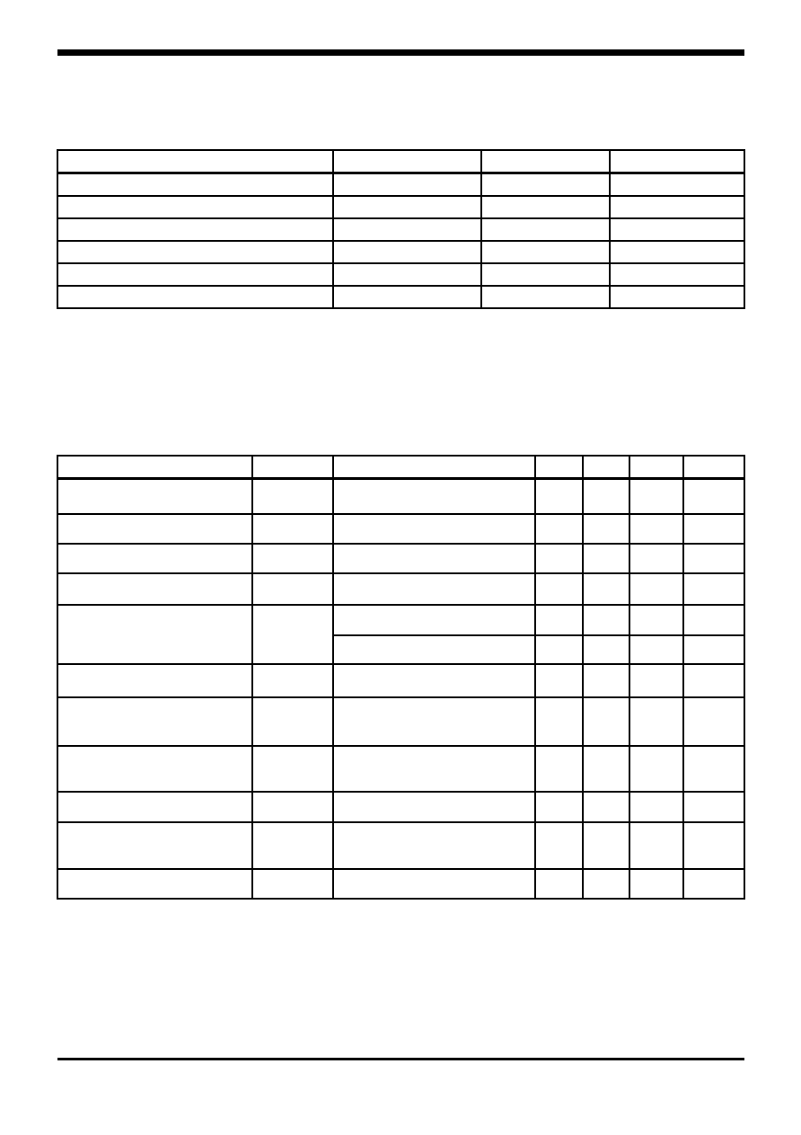
Absolute maximum ratings
(Ta =
2
5
∞C
)
Characteristic Symbol
Ratings
Unit
Supply voltage
V
CC
±
18 V
Differential input voltage
V
ID
±
30 V
Input voltage
V
IC
-Vcc~Vcc V
Power Dissipation
P
D
800
mW
Operating temperature
T
opr
-40 ~ +85
∞C
Storage temperature
T
stg
-55 ~ +125
∞C
* Refer to Pd characteristics diagram. The values for the S4560 are those when it is mounted on a glass epoxy
PCB(50 ◊50 ◊1.6 ).
Electrical Characteristics
(Unless otherwise specified. V
CC
= +15V, V
EE
=15V and Ta =
2
5
∞C
)
Characteristic Symbol Test
Condition Min.
Typ.
Max.
Unit
Input offset voltage
V
IOS
Rg 10
- 0.5 6 mV
Input offset current
I
IOS
-
-
5
200
nA
Input bias current
I
IB
-
-
50
500
nA
Input common mode
Voltage Range
V
ICR
-
±
12
±
14
- V
R
L
10
±
12
±
14
- V
Maximum Output Voltage
V
OM
R
L
2
±
10
±
13
- V
Large signal Voltage Gain
G
V
Vout=±10V, RL 2
86 100 -
dB
Common mode
rejection ratio
CMRR
Rg 10
70 90 - dB
Power supply
rejection ratio
PSRR
Rg 10
- 30 150 uV/V
Slew Rate
SR
G
V
=1, R
L
2
- 4.0 - V/us
Input conversion
noise voltage
V
n
-
-
-
2.2
uV
Gain band width product
GBW
f=10kHz
-
10
-
MHz
