 | –≠–ª–µ–∫—Ç—Ä–æ–Ω–Ω—ã–π –∫–æ–º–ø–æ–Ω–µ–Ω—Ç: S72N42N | –°–∫–∞—á–∞—Ç—å:  PDF PDF  ZIP ZIP |

KSD-I0C002-000
1
S72NxxN
Standard Voltage Detector
7
Description
The function of this low reset Type IC is to accurately reset systems after detecting the supply voltage at the time
of switching power on and instantaneous power off in various CPU and other logic system. Further, this IC, with
its super low consumption current is most suited as a voltage check circuit for a number of products which use
batteries.
Features
∑ Super low current consumption (I
CCL
= 1.0uA Typ.)
∑ High current of output transistor (I
OL
=20mA Typ.)
∑ Hysteresis circuit built in (V
S
=100mV Typ.)
∑ It has on delay function to supplement the constant of outer C and R.
Applications
∑ Reset circuits for microcomputers, CPU and MPU.
∑ Reset circuit for logic circuitry.
∑ Battery voltage check circuit.
∑ Circuit for changing over to backup battery.
∑ Level detecting circuit.
Ordering Information
Type NO.
Marking
Package Code
S72NxxN
S72N
TO-92N
: Detecting Voltage Code
Outline Dimensions
Unit : mm
S
S
e
e
m
m
i
i
c
c
o
o
n
n
d
d
u
u
c
c
t
t
o
o
r
r
PIN Connections
1. OUT
2. Vcc
3. GND
0.90 M ax.
1.27 Typ.
3
.
0
9
~
3
.
2
9
3.55 Typ
0.72 M ax.
0.52 M ax.
4
.
2
0
~
4
.
4
0
4.20~4.40
1
3
.
5
0
~
1
4
.
5
0
2
.
1
4
T
y
p
.
0.40 M ax.
2.25 M ax.
1 2 3
KSD-I0C002-000
2
S72NxxN
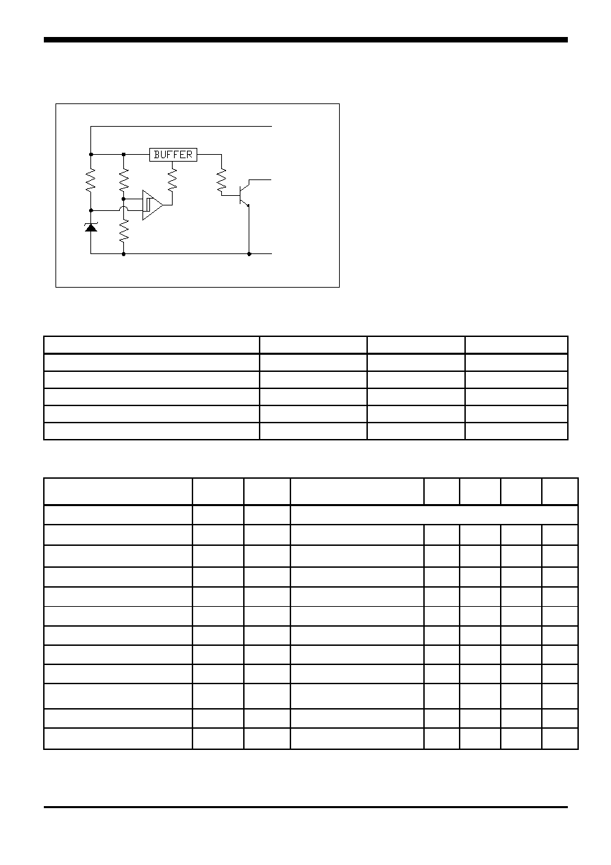
Equivalent Circuit Diagram
Maximum ratings
(Ta=25
∞C)
Characteristic Symbol
Ratings
Unit
Supply Voltage
V
CC
-0.3 ~ +10
V
Power Dissipation
P
D
500
mW
Output Voltage
V
OUT
-0.3 ~ +10
V
Operating Temperature Range
T
OPR
-20 ~ +75
Storage Temperature Range
T
STG
-40 ~ +125
Electrical Characteristics
(V
CC
=5V, Ta=25
∞C)
Characteristic Symbol
Test
Circuit
Test Condition
Min.
Typ.
Max.
Unit
Detecting Voltage
V
S
1
* See Table 1
Hysteresis Voltage
V
S
1
R
L
=470, V
CC
= LHL
40 100 300 mV
Temperature Coefficient
of Detecting Voltage
V
S
/T
1
R
L
=470, Ta= -20~75
-
±
0.01
-
%/
Low Level Output voltage
V
OL
1
R
L
=470, V
CC
= V
S
Min
- 0.1 0.4 V
Leakage Current When OFF
I
LEAK
1
V
CC
=10V, R
L
=470
- - 0.1
µA
Circuit current at ON
I
CCL
1
V
CC
= V
S
Min
-
100
180
µA
Circuit current at OFF
I
CCH
1
V
CC
= V
S
Max +0.1V
-
1.0
2.5
µA
Operating Voltage
V
OPR
1
R
L
=4.7 , V
OL
0.4V
- 1.4 1.6 V
Output Current at ON I
I
OL
I 1
R
L
=0, V
CC
= V
S
Min
10 20 - mA
Output Current at ON II
I
OL
II 1
R
L
=0, V
CC
= V
S
Min,
Ta= -20~75
5 - - mA
LH Transmission delay time
t
PLH
2
R
L
=4.7 , C
L
=100
- 100 500
HL Transmission delay time
t
PHL
2
R
L
=4.7 , C
L
=100
- 10 20
V
S
: Standard Detection Voltage
Vcc
OUT
GND

KSD-I0C002-000
3
S72NxxN
* Table 1
Electrical Characteristics
(V
CC
=5V, Ta=25
∞C)
Characteristic Symbol
Test
Circuit
Test Condition
Min.
Typ. Max.
Unit
S72N45N 4.30 4.50 4.70
S72N42N 4.00 4.20 4.40
S72N39N 3.70 3.90 4.10
S72N36N 3.40 3.60 3.80
S72N33N 3.10 3.30 3.50
S72N31N 2.90 3.10 3.30
S72N29N 2.75 2.90 3.05
S72N27N 2.55 2.70 2.85
S72N25N 2.35 2.50 2.65
Detecting voltage
V
S
1
R
L
=470
V
CC
=HL
V
OL
0.4V
S72N23N 2.15 2.30 2.45
V

KSD-I0C002-000
4
S72NxxN
(1) Battery Low Indicator
Test Circuit 2
Application Circuit
Test Circuit 1
(2) Resetting for CPU
Note 1.
: Connecting of LED and R2
obtains a voltage drop indicator.
Note 2.
: Connecting of C1 and selection of time constant
with C1 and R1 set the power on delay time.

KSD-I0C002-000
5
S72NxxN
Electrical Characteristic Curves
Fig. 4 V
S
≠ T
a
Fig. 6 V
OL
≠ T
a
Fig. 1 V
O
≠ V
CC
Fig. 2 I
CC
≠ V
CC
Fig. 5 I
CCL
≠ T
a
Fig. 3 V
S
≠ T
a