 | –≠–ª–µ–∫—Ç—Ä–æ–Ω–Ω—ã–π –∫–æ–º–ø–æ–Ω–µ–Ω—Ç: S7809D | –°–∫–∞—á–∞—Ç—å:  PDF PDF  ZIP ZIP |

KSI-2009-004
1
S78xxD
Fixed Voltage Regulator
Descriptions
The S78xx series are three-terminal positive regulators providing over 1A output current
with internal current limiting, thermal shutdown and safe area protection. These regulators
are useful in a wide range of applications. Although they are just fixed voltage regulators,
the S78xx series can be used with external components to obtain adjustable voltages and
currents.
Features
∑ Internal Short Circuit Current Limiting
∑ Maximum Output Current (1A Max.)
∑ Thermal Overload Protection
∑ Output Transistor Safe Area Protection
Ordering
Information
Type NO. Marking Package Code
S78xxD S78D D-Pak
:Voltage Code (05:5V, 06:6V, 08:8V, 09:9V, 10:10V,12:12V,15:15V,24:24V)
Outline Dimensions unit :
mm
S
S
e
e
m
m
i
i
c
c
o
o
n
n
d
d
u
u
c
c
t
t
o
o
r
r
PIN Connections
1. Input
2. GND
3. Output

KSI-2009-004
2
S78xxD
Absolute Maximum Ratings
Ta=25
∞C
Characteristic Symbol
Ratings Unit
40 (S7824D)
V
Operating Input voltage
V
IN
35 (ALL Others)
V
Power Dissipation (without Heatsink)
P
D
1.3 W
Operating Junction Temperature
T
J
-30 ~ 125
∞C
Storage Temperature
T
stg
-55 ~ 150
∞C
Electrical Characteristics
(V
IN
= 10V, I
OUT
= 500mA, T
j
= 0
∞C ~ 125∞C, Unless otherwise noted)
S7805D
Characteristic Symbol Test
Condition
Min. Typ. Max.
Unit
T
j
=25
4.8 5.0 5.2
Output Voltage
V
OUT
I
OUT
=5mA ~ 1A
V
IN
=7.0V ~ 20V, P
O
15W
4.75 5.0 5.25
V
V
IN
=7.0V ~ 25V
-
3
100
Line Regulation
V
OUT
V
IN
=8.0V ~ 12V
T
j
=25
- 1 50
mV
I
OUT
=5mA ~ 1.5A
-
15
100
Load Regulation
V
OUT
I
OUT
=250mA ~ 750mA
T
j
=25
- 5 50
mV
Quiescent Current
I
B
T
j
=25
- 4.2 8.0 mA
V
IN
= 7.0V ~ 25
V
- - 1.3
Quiescent Current Change
I
B
I
OUT
= 5mA ~ 1A
-
-
0.5
mA
Output Noise Voltage
V
N
f=10Hz ~ 100KHz
T
j
=25
- 40 -
uV
rms
Ripple Rejection Ratio
RR
f=120
Hz,
V
IN
=8.0V ~ 18
V
62 78 - dB
Dropout Voltage
V
D
I
OUT
=1A
T
j
=25
- 2.0 - V
Short Circuit Current Limit
I
SC
T
j
=25
- 0.75 - A
Output Voltage Drift
TC
VO
I
OUT
=5mA
T
j
=25
- -1.1 - mV/
∞C
Peak Output Current
I
PK
T
j
=25
- 2.2 - A
Pulse testing techniques are used to maintain the junction temperature as close to the ambient
temperature as possible. Thermal effects must be taken into separately.

KSI-2009-004
3
S78xxD
Electrical Characteristics
(V
IN
= 11V, I
OUT
= 500mA, T
j
= 0
∞C ~ 125∞C, Unless otherwise noted)
S7806D
Characteristic Symbol Test
Condition
Min. Typ. Max.
Unit
T
j
=25
5.75 6.0 6.25
Output Voltage
V
OUT
I
OUT
=5mA ~ 1A
V
IN
=8.0V ~ 21V, P
O
15W
5.7 6.0 6.3
V
V
IN
=8.0V ~ 25V
-
5
120
Line Regulation
V
OUT
V
IN
=9.0V ~ 13V
T
j
=25
- 1.5 60
mV
I
OUT
=5mA ~ 1.5A
-
14
120
Load Regulation
V
OUT
I
OUT
=250mA ~ 750mA
T
j
=25
- 4 60
mV
Quiescent Current
I
B
T
j
=25
- 4.3 8.0 mA
V
IN
= 8.0V ~ 25
V
- - 1.3
Quiescent Current Change
I
B
I
OUT
= 5mA ~ 1A
-
-
0.5
mA
Output Noise Voltage
V
N
f=10Hz ~ 100KHz
T
j
=25
- 45 -
uV
rms
Ripple Rejection Ratio
RR
f=120
Hz,
V
IN
=9.0V ~ 19
V
59 75 - dB
Dropout Voltage
V
D
I
OUT
=1A
T
j
=25
- 2.0 - V
Short Circuit Current Limit
I
SC
T
j
=25
- 0.55 - A
Output Voltage Drift
TC
VO
I
OUT
=5mA
T
j
=25
- -0.8 - mV/
∞C
Peak Output Current
I
PK
T
j
=25
- 2.2 - A
Pulse testing techniques are used to maintain the junction temperature as close to the ambient
temperature as possible. Thermal effects must be taken into separately.

KSI-2009-004
4
S78xxD
Electrical Characteristics
(V
IN
= 14V, I
OUT
= 500mA, T
j
= 0
∞C ~ 125∞C, Unless otherwise noted)
S7808D
Characteristic Symbol Test
Condition
Min. Typ. Max.
Unit
T
j
=25
7.7 8.0 8.3
Output Voltage
V
OUT
I
OUT
=5mA ~ 1A
V
IN
=10.5V ~ 23V, P
O
15W
7.6 8.0 8.4
V
V
IN
=10.5V ~ 25V
-
6
160
Line Regulation
V
OUT
V
IN
=11.0V ~ 17V
T
j
=25
- 2 80
mV
I
OUT
=5mA ~ 1.5A
-
12
160
Load Regulation
V
OUT
I
OUT
=250mA ~ 750mA
T
j
=25
- 4 80
mV
Quiescent Current
I
B
T
j
=25
- 4.3 8.0 mA
V
IN
= 10.5V ~ 25
V
- - 1.0
Quiescent Current Change
I
B
I
OUT
= 5mA ~ 1A
-
-
0.5
mA
Output Noise Voltage
V
N
f=10Hz ~ 100KHz
T
j
=25
- 52 -
uV
rms
Ripple Rejection Ratio
RR
f=120
Hz,
V
IN
=11.5V ~ 21.5
V
55 72 - dB
Dropout Voltage
V
D
I
OUT
=1A
T
j
=25
- 2.0 - V
Short Circuit Current Limit
I
SC
T
j
=25
- 0.45 - A
Output Voltage Drift
TC
VO
I
OUT
=5mA
T
j
=25
- -0.8 - mV/
∞C
Peak Output Current
I
PK
T
j
=25
- 2.2 - A
Pulse testing techniques are used to maintain the junction temperature as close to the ambient
temperature as possible. Thermal effects must be taken into separately.
KSI-2009-004
5
S78xxD
Electrical Characteristics
(V
IN
= 16V, I
OUT
= 500mA, T
j
= 0
∞C ~ 125∞C, Unless otherwise noted)
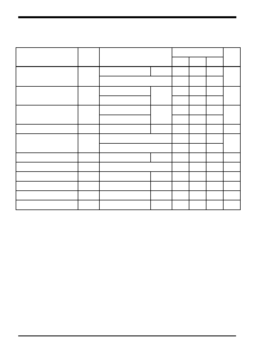
S7809D
Characteristic Symbol Test
Condition
Min. Typ. Max.
Unit
T
j
=25
8.65 9.0 9.35
Output Voltage
V
OUT
I
OUT
=5mA ~ 1A
V
IN
=11.5V ~ 24V, P
O
15W
8.55 9.0 9.45
V
V
IN
=11.5V ~ 27V
-
7
180
Line Regulation
V
OUT
V
IN
=13.0V ~ 19V
T
j
=25
- 2 90
mV
I
OUT
=5mA ~ 1.5A
-
12
180
Load Regulation
V
OUT
I
OUT
=250mA ~ 750mA
T
j
=25
- 4 90
mV
Quiescent Current
I
B
T
j
=25
- 4.3 8.0 mA
V
IN
= 11.5V ~ 27
V
- - 1.0
Quiescent Current Change
I
B
I
OUT
= 5mA ~ 1A
-
-
0.5
mA
Output Noise Voltage
V
N
f=10Hz ~ 100KHz,
T
j
=25
- 60 -
uV
rms
Ripple Rejection Ratio
RR
f=120
Hz,
V
IN
=12V ~ 22
V
55 70 - dB
Dropout Voltage
V
D
I
OUT
=1A
T
j
=25
- 2.0 - V
Short Circuit Current Limit
I
SC
T
j
=25
- 0.4 - A
Output Voltage Drift
TC
VO
I
OUT
=5mA
T
j
=25
- -1.0 - mV/
∞C
Peak Output Current
I
PK
T
j
=25
- 2.2 - A
Pulse testing techniques are used to maintain the junction temperature as close to the ambient
temperature as possible. Thermal effects must be taken into separately.