KST-9018-000
1
STS9015
PNP Silicon Transistor
Description
∑
General purpose application.
∑
Switching application.
Features
∑
Excellent h
FE
linearity : h
FE
(I
C
=0.1mA) / h
FE
(I
C
=2mA) = 0.95(Typ.)
∑
Low noise : NF = 10dB(Max.)
∑
Complementary pair with STS9014
Ordering
Information
Type NO. Marking Package Code
STS9015 STS9015 TO-92
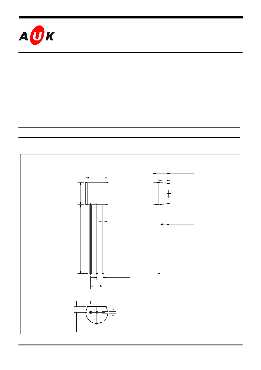
Outline Dimensions unit : mm
S
S
e
e
m
m
i
i
c
c
o
o
n
n
d
d
u
u
c
c
t
t
o
o
r
r
4.5
±
0.1
4.
5
±
0.
1
0.4
±
0.02
1.27 Typ
.
2.54 Typ
.
1 2 3
3.45
±
0.1
2.25
±
0.1
2.06
±
0.1
1.
2
0
±
0.
1
0.
3
8
PIN Connections
1. Emitter
2. Base
3. Collector
14.
0
±
0.
40
KST-9018-000
2
STS9015
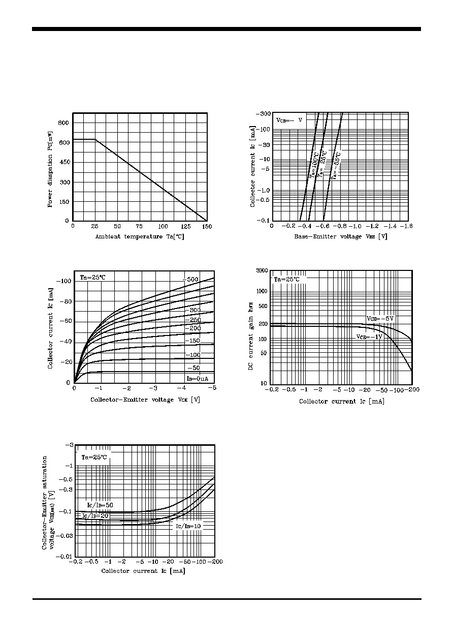
Absolute maximum ratings
(Ta=25
∞
∞
∞
∞
C)
Characteristic
Symbol
Ratings
Unit
Collector-Base voltage
V
CBO
-50
V
Collector-Emitter voltage
V
CEO
-50
V
Emitter-Base voltage
V
EBO
-5
V
Collector current
I
C
-150
mA
Emitter current
I
E
150
mA
Collector dissipation
P
C
625
mW
Junction temperature
T
j
150
∞
C
Storage temperature
T
stg
-55~150
∞
C
Electrical Characteristics
(Ta=25
∞
∞
∞
∞
C)
Characteristic
Symbol
Test Condition
Min. Typ. Max.
Unit
Collector cut-off current
I
CBO
V
CB
=-50V, I
E
=0
-
-
-50
nA
Emitter cut-off current
I
EBO
V
EB
=-5V, I
C
=0
-
-
-100
nA
DC current gain
h
FE
*
V
CE
=-5V, I
C
=-1mA
100
-
1000
-
Collector-Emitter saturation voltage
V
CE(sat)
I
C
=-100mA, I
B
=-10mA
-
-0.1
-0.3
V
Transition frequency
f
T
V
CE
=-10V, I
C
=-1mA
60
-
-
MHz
Collector output capacitance
C
ob
V
CB
=-10V, I
E
=0, f=1MHz
-
4
7
pF
Noise figure
NF
V
CE
=-6V, I
C
=-0.1mA
f=1KHz, Rg=10K
-
-
10
dB
*: h
FE
rank / B : 100~300, C : 200~600, D : 400~1000.