KLB-9001-002
1
SB5311 / SB5311(B)
LED Lamp
Features
· Colorless transparency lens type
· 5mm(T-13/4) all plastic mold type
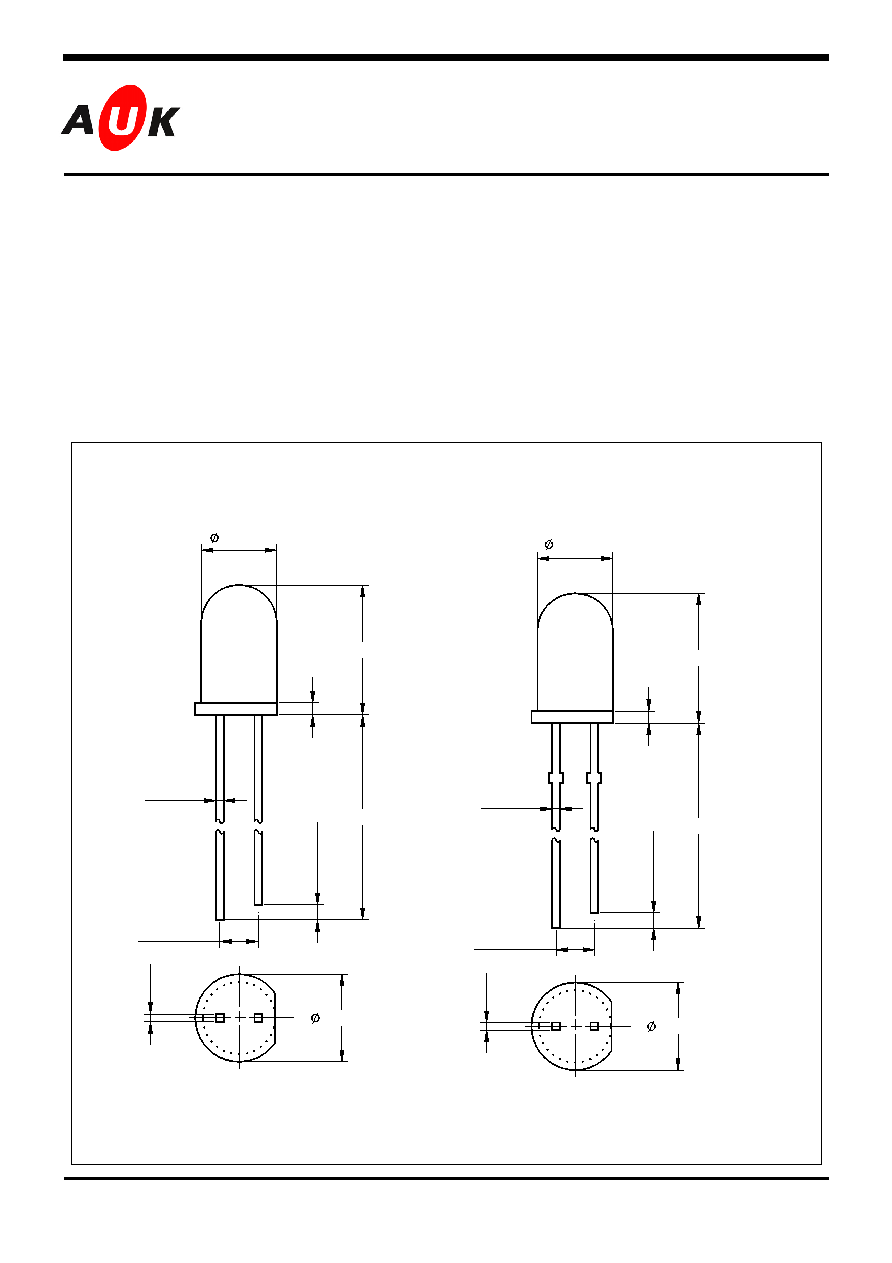
Outline Dimensions unit :
mm
STRAIGHT TYPE STOPPER TYPE
8.6±
0.2
5.8±
0.2
1
.
0
M
I
N
1
.
0
M
I
N
5.8±
0.2
0
.
5
1
2
2.54NOM
0
.
5
1
2
2.54NOM
8.6±
0.2
0.5
23.0 MIN
0.8±
0.2
0.5
0.8±
0.2
5.0±
0.2
5.0±
0.2
PIN Connections
1.Anode
2.Cathode
S
S
e
e
m
m
i
i
c
c
o
o
n
n
d
d
u
u
c
c
t
t
o
o
r
r
KLB-9001-002
2
SB5311 / SB5311(B)
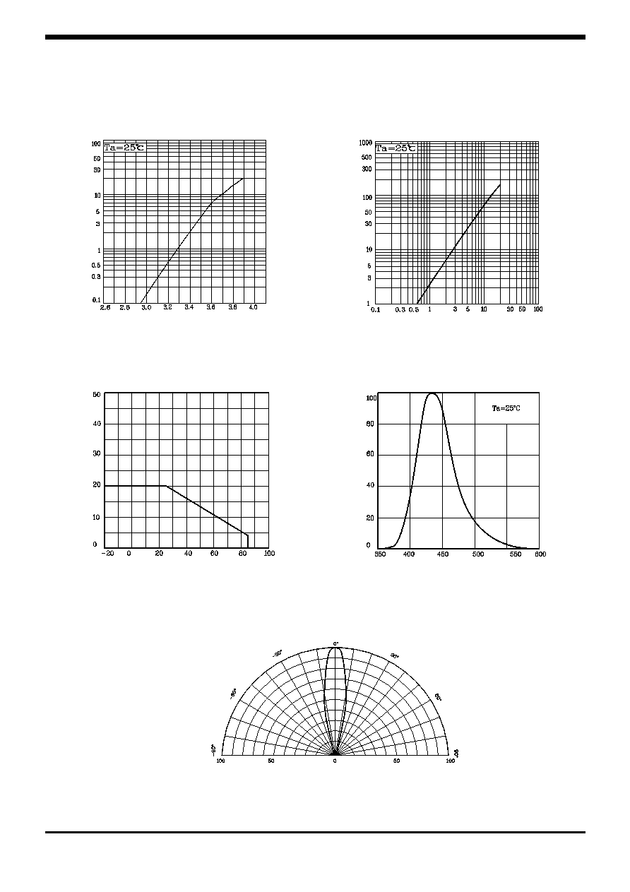
Absolute maximum ratings
Characteristic Symbol
Ratings
Unit
Power Dissipation
P
D
85
mW
Forward Current
I
F
20
mA
*
1
Peak Forward Current
I
FP
50
mA
Reverse Voltage
V
R
4
V
Operating Temperature
T
opr
-2585
Storage Temperature
T
stg
-30100
*
2
Soldering Temperature
T
sol
260 for 5 seconds
*1.Duty ratio = 1/16, Pulse width = 0.1ms
*2.Keep the distance more than 2.0mm from PCB to the bottom of LED package
Electrical Characteristics
Characteristic Symbol
Test
Condition
Min.
Typ.
Max.
Unit
Forward Voltage
V
F
I
F
= 10mA
-
3.7
4.2
V
Luminous Intensity
I
V
I
F
= 10mA
30
75
-
mcd
Peak Wavelength
P
I
F
= 10mA
-
435
-
nm
Spectrum Bandwidth
I
F
= 10mA
-
60
-
nm
Reverse Current
I
R
V
R
=4V -
-
10
uA
*
3
Half angle
1/2
I
F
= 10mA
-
±11
- deg
*3.
1/2
is the off-axis angle where the luminous intensity is 1/2 the peak intensity