 | –≠–ª–µ–∫—Ç—Ä–æ–Ω–Ω—ã–π –∫–æ–º–ø–æ–Ω–µ–Ω—Ç: SD60C32P | –°–∫–∞—á–∞—Ç—å:  PDF PDF  ZIP ZIP |

KSI-W015-000
1
SD60C32/P, SD60C52/P
CMOS SINGLE-COMPONENT 8-BIT MICROCOMPUTER
Description
The AUK 60C32/P 60C52/P is a high-performance micro controller fabricated with AUK
high-density CMOS technology. The AUK CMOS technology combines the high speed and
density characteristics of MOS with the low power attributes of CMOS.
The 60C52 contains a 8K◊8 ROM, a 256◊8 RAM, 32 I/O lines, three 16bit counter/timers,
a six sourc two-priority level nested interrupt structure, a serial I/O port for either multi-
processor communication, I/O expansion or full duplex UART, and on-chip oscillator and
clock circuits.
In addition, the device has two software selectable modes of power reduction idle mode
and power-down mode. The idle mode freezes the CPU while allowing the RAM, timers,
serial port, and interrupt system to continue functioning.
The power-down mode saves the RAM contents but freezes the oscillator , causing all other
chip function to be inoperative.
Features
∑
8-bit CPU optimized for control applications.
∑
MCS-51 fully compatible instruction set
∑
Pin-to-pin compatible with intel's 80C52/80C32.
∑
ONCE
TM
(ON-circuit emulation) mode
∑
256 Bytes of on-chip data RAM.
∑
Power control modes
∑
60C52 low power CPU only. -Idle mode
∑
32 programmable I/O lines. -Power down mode
∑
Three 16bit timer/counters.
∑
6 interrupt source
∑
TTL and CMOS compatible logic levels
∑
64K external program memory space and data memory space
.
Ordering Information
Type NO.
Marking
Package Code
Type NO.
Marking
Package Code
SD60C32
SD60C32
PLCC44
SD60C32P
SD60C32
DIP40
SD60C52
SD60C52
PLCC44
SD60C52P
SD60C52
DIP40
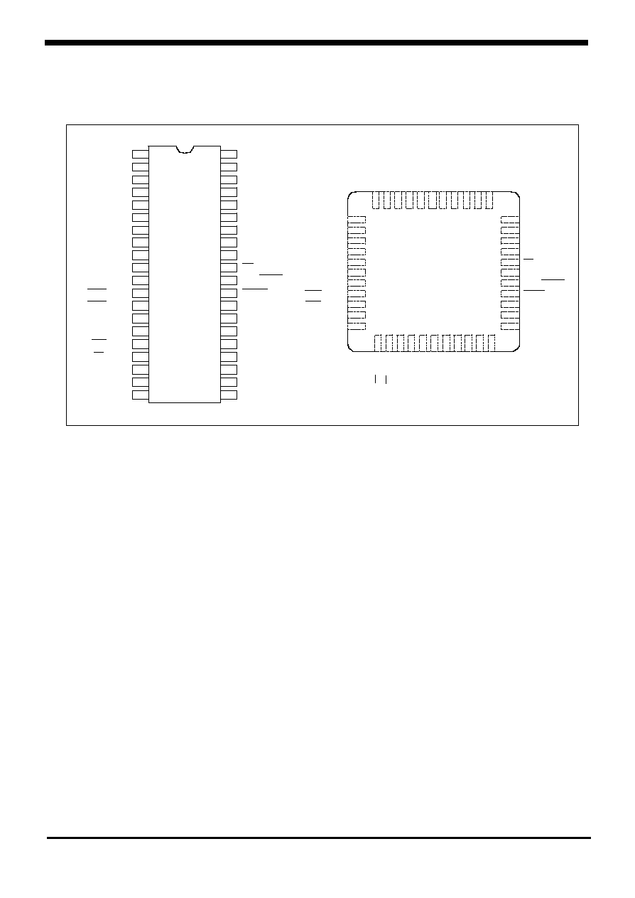
Outline Dimensions
unit : mm
S
S
e
e
m
m
i
i
c
c
o
o
n
n
d
d
u
u
c
c
t
t
o
o
r
r
0.120 (3.048)
0.090 (2.286)
0.048 (1.219)
0.042(1.067) 45
o
0.695 (17.653)
0.685 (17.399)
0.656 (16.662)
0.650 (16.510)
0.695 (17.653)
0.685 (17.399)
0.656 (16.662)
0.650 (16.510)
0.050 (1.270)
0.630 (16.002)
0.590 (14.906)
SEATING PLANE
MIN 0.020 (0.508)
BASE PLANE
0.180 (4.572)
0.165 (4.191)
40
21
1
20
13.4 0.2
15.24
1
5 M A X
0.25
1.22TYP
2 . 5 4
1 . 4 0 . 1
0 . 5 0 . 1
0.5MIN
4.5 0.3
3.5 0.3
50.7±0.2
±
±
±
±
±
±
PLCC44 DIP40

KSI-W015-000
2
Absolute Maximum Ratings
Characteristic
Rating
Unit
Ambient temperature under bias
0 ~ +70
Storage temperature
- 65 ~ + 150
Voltage on any pin to V
SS
- 0.5 ~ V
CC
+ 0.5
V
Maximum I
OL
per I/O pin
15
Power dissipation
1.5
W
Block Diagram
SD60C32/P SD60C52/P
Vcc
Vss
RAM ADDR
REGISTER
RAM
PORT 0
LATCH
PORT 2
LATCH
PORT 0
DRIVERS
P0.0-P0.7
P2.0-P2.7
PORT 2
DRIVERS
ROM/
EPROM
B
REGISTER
ACC
STACK
POINTER
TMP2
TMP1
ALU
PSW
PSEN
ALE
EA
RST
TIMING
AND
CONTROL
REGISTER
PORT 1
LATCH
PCON
SCON TMOD
TCON
T2CON
TH0
TL0
TL1
TH1
TH2
TL2
RCAP2H
RCAP2L
SBUF
IE
PORT 1
DRIVERS
IP
PORT AND TIMER BLOCKS
INTERRUPT SERIAL
PORT 3
LATCH
PORT 3
DRIVERS
OSCILLATOR
P1.0-P1.7
XTAL1
XTAL2
PD
P3.0-P3.7
PROGRAM
ADDRESS
REGISTER
BUFFER
PC
INCRE-
MENTER
PROGRAM
COUNTER
DPTR
INSTRUCTION
KSI-W015-000
3
Pin Configuration
Pin Description
V
CC
: PIN 40 (DIP40), PIN 44 (PLCC44)
Supply voltage during normal, Idle and power down operations.
V
SS
: PIN 20 (DIP 40), PIN 22 (PLCC44)
Circuit ground.
Port 0 : PIN 32~39 (DIP 40), PIN 36~43 (PLCC44)
Port 0 is an 8bit open drain bi-directional I/O port. As an output
port each pin can sink several LS TTL inputs. Port 0 pins that have 1's
written to them float, and in that state can be used as high impedance inputs.
Port 0 is also the multiplexed low-order address and data bus during accesses
to external program and data memory.
In this application it uses strong internal pullups when emitting 1's and source and
sink several LS TTL inputs. Port 0 outputs the code bytes during program verification
on the 60C52 external pullups resistors are required during program verification.
Port 1 : PIN 1~8 (DIP 40), PIN 2~9 (PLCC44)
Port 1 output buffers can drive LSI TTL inputs.
Port 1 is an 8bit bi-directional I/O port with internal pullups.
Port 1 pins that have 1's written to them are pulled high by the internal pullups,
and in that state can be used as inputs. As inputs, Port 1 pins that are externally
being pulled low will source current because of the internal pullups
SD60C32/P SD60C52/P
44PLCC
7
8
9
10
12
11
13
14
15
16
17
39
38
37
36
34
35
33
32
31
30
29
18
19
20
21
23
22
24
25
26
27
28
P1.5
P1.6
P1.7
RST
RxD/P3.0
NC
TxD/3.1
INT0/P3.2
INT1/P3.3
T0/P3.4
T1/P3.5
P0.4/AD4
P0.5/AD5
P0.6/AD6
P0.7/AD7
EA/V
PP
NC
ALE/PROG
PSEN
P2.7/A15
P2.6/A14
P2.5/A13
WR/P3.6
RD/P3.7
XTAL2
XTAL1
V
SS
NC
A8/P2.0
A9/P2.1
A10/P2.2
A11/P2.3
A12/P2.4
P1.4
P1.3
P1.2
P1.1/T2EX
P1.0/T2
NC
V
CC
P0.0/AD0
P0.1/AD1
P0.2/AD2
P0.3/AD3
40DIP
T2/P1.0
T2EX/P1.1
P1.2
P1.3
P1.4
P1.5
P1.6
P1.7
RST
RxD/P3.0
INT0/P3.2
TxD/P3.1
INT1/P3.3
T0/P3.4
T1/P3.5
WR/P3.6
RD/P3.7
XTAL2
XTAL1
V
SS
1
2
3
4
5
6
7
8
9
10
11
12
13
14
15
16
17
18
19
20
40
39
38
37
36
35
34
33
32
31
30
29
28
27
26
25
24
23
22
21
V
C C
P0.0/AD0
P0.1/AD1
P0.2/AD2
P0.3/AD3
P0.4/AD4
P0.5/AD5
P0.6/AD6
P0.7/AD7
EA/V
P P
PSEN
ALE/PROG
P2.7/A15
P2.6/A14
P2.5/A13
P2.4/A12
P2.3/A11
P2.2/A10
P2.1/A9
P2.0/A8
6
5
4
3
1
2
44
43
42
41
40

KSI-W015-000
4
Pin Description (Continued)
In addition, Port 1 serves the functions of the following special features of the 60C52.
Port Pin
Alternate Function
P1.0
T2(External Count Input to Timer / Counter 2)
P1.1
T2EX(Timer / Counter 2 Capture/Reload Trigger and Direction Control)
Port 1 receives the low-order address bytes during ROM verification.
Port 2
: PIN 21~28 (40DIP), PIN 24~31 (44PLCC)
Port 2 is an 8-bit bi-directional I/O port with internal pullups. The port 2 output buffers can
drive LS TTL inputs.
Port 2 pins that have 1's written to them are pulled high by the internal pullups, and in
that state can be used as input.
As inputs, port 2 pins that are externally being pulled
low will source current because of the internal pullups.
Port 2 emits the high-order address byte during fetches from external Program Memory
and during accesses to external data memory that use 16-bit addresses (MOVX @ DPTR).
In this application it uses strong internal pullups when emitting 1s. During accesses to
external data memory that use 8 bit addresses (MOVX @ Ri), port 2 emits the contents
of the P2 special function register
Port 3 : PIN 10~17 (DIP 40), PIN 13~19 (PLCC44)
Port 3 is an 8bit bi-directional I/O port with internal pullups. The port 3 output buffers can
drive LS TTL input. Port 3 pins that have 1's written to them are pulled high by the internal
pullups, and in that state can be used as inputs. As inputs, Port 3 pins that are externally
being pulled low will source current because of the pullups.
Port 3 also serves the function of various special feature of the MCS-51 Family,
as listed below :
Port PIN
PIN NO.
Alternate Function
P3.0
10
RxD (Serial input port)
P3.1
11
TxD (Serial output port)
P3.2
12
INT0 (External interrupt 0)
P3.3
13
INT1 (External interrupt 1)
P3.4
14
T0 (Timer 0 external input)
P3.5
15
T1 (Timer 1 external input)
P3.6
16
WR (External data memory write strobe)
P3.7
17
RD (External data memory read strobe)
SD60C32/P SD60C52/P
KSI-W015-000
5
RST: PIN 9 (DIP40), PIN 10 (PLCC44)
Reset input. A high on this pin for two machine cycles while the oscillator is running
resets the device. An internal pulldown resistor permits a power-on reset with
only a capacitor connected to V
CC
.
ALE: PIN 30 (DIP40), PIN 33 (PLCC44)
Address latch enable output pulse for latching the low byte of the address
during accesses to external memory.
In normal operation ALE is emitted at a constant rate of 1/6 the oscillator frequency,
and may be used for external timing or clocking purposes.
Note : However, that one ALE pulse is skipped during each access to external
data memory.
This pin is also the program pulse input PROG during EPROM programming.
PSEN : PIN 29 (DIP 40), PIN 32 (PLCC44)
Program store enable is the read strobe to external program memory. When the 60C52
is executing code from external program memory, PSEN is activated twice each machine
cycle, except that two PSEN activations are skipped during each access to external
data memory. PSEN is not activated during fetches from internal program memory.
EA: PIN 31 (DIP 40), PIN 35 (PLCC44)
External access enable. EA must be strapped to V
SS
in order to enable the device
to fetch code from external program memory locations starting at 0000H up to FFFFH.
If EA is strapped to V
CC
the device executes from internal program memory unless
the program counter contains an address greater than 0FFFH.
XTAL1: PIN 19 (DIP 40), PIN 21 (PLCC44)
Input to the Inverting oscillator amplifier and input to the internal clock generator circuits.
XTAL2: PIN 18 (DIP 40), PIN 20 (PLCC44)
Output from the inverting oscillator amplifier
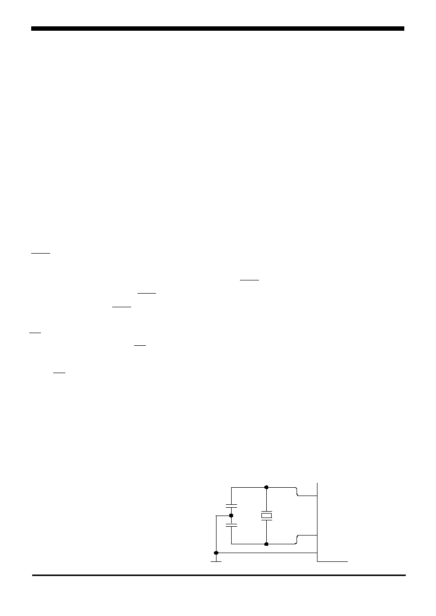
0 Crystal Oscillator
NC: PIN1, 12, 23, 34 (PLCC44)
Non connection pins.
30pF
30pF
V
SS
XTAL1
XTAL2
SD60C32/P SD60C52/P

KSI-W015-000
6
Idle Mode
In the Idle mode, the CPU puts itself to sleep while all the on chip peripherals stay active.
The instruction that invokes the Idle mode is the last instruction executed in the normal
operating mode before Idle mode is activated.
The content of the on-chip RAM and all the special function registers remain intact during
this mode. The Idle mode can be terminated either by any enabled interrupt, at which time the
process is picked up at the interrupt service routine and continued, or by a hardware reset
which starts the processor the same as a power on reset.
Power Down Mode
In the power down mode the oscillator is stopped, and the instruction that invokes power
down is the last instruction executed. The on-chip RAM and special function register
retain their values until the power down mode is terminated.
The only exit from power down is a hardware reset. Reset redefines the SFRs but does
not change the on-chip RAM. The reset should not be activated before V
CC
is restored
to its normal operating level and must be held active long enough to allow the oscillator to
restart and stabilize.
The control bits for the reduced power modes are in the special function register PCON.
Table. Status of the external pins during Idle and power down modes.
Mode
Program
Memory
ALE
PSEN
PORT 0 PORT 1 PORT 2 PORT 3
Idle
Internal
1
1
Data
Data
Data
Data
Idle
External
1
1
Float
Data
Address
Data
Power
Down
Internal
0
0
Data
Data
Data
Data
Power
Down
External
0
0
Float
Data
Data
Data
SD60C32/P SD60C52/P

KSI-W015-000
7
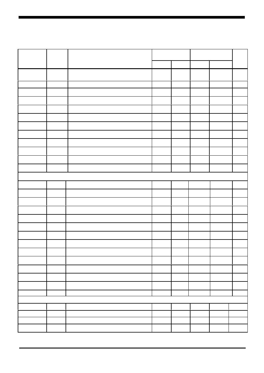
Electrical Characteristics (DC)
(T
a
= 0 ~ 70 or -40 ~ 85, V
CC
= 5V ± 20%, V
SS
=0V)
LIMITS
SYMBOL
PARAMETER
TEST
CONDITIONS MIN TYP. MAX
UNIT
V
IL
Input low voltage, except EA
-0.5
0.2V
CC
-
0.1
V
V
IL1
Input low voltage to EA
0
0.2V
CC
-
0.3
V
V
IH
Input high voltage, except
XTAL1,RST
0.2V
CC
+0.9
V
CC
+0.5
V
V
IH1
Input high voltage to XTAL1, RST
0.7 V
CC
V
CC
+0.5
V
V
OL
Output low voltage to ports 1,2,3
I
OL
=1.6
0.45
V
V
OL1
Output low voltage to ports 0,
ALE, PSEN
I
OL
=3.2
0.45
V
V
OH
Output high voltage to ports
1,2,3,ALE,PSEN
I
OH
=-60
I
OH
=-30
I
OH
=-10
V
CC
-0.3
V
CC
-0.7
V
CC
-1.5
V
V
OH1
Output high voltage
(port 0 in external bus mode)
I
OH
=-200
I
OH
=-3.2
I
OH
=-7.0
V
CC
-0.3
V
CC
-0.7
V
CC
-1.5
V
I
IL
Logical 0 input current to ports
1,2,3
V
IN
=0.45V
-10
-50
I
TL
Logical 1 to 0 transition current to
ports 1,2,3
VI
N
=2V
- 265
-650
I
LI
Input leakage current to port 0, EA
0 < V
I N
< V
CC
0.02
±
10
I
CC
Power supply current
Active mode @ 12MHz
Idle mode @ 12MHz
Power-down mode
15
5
5
30
7.5
75
R
RST
Internal reset pull-down resistor
40
100
225
kohm
C
1O
Pin capacitance
10
pF
SD60C32/P SD60C52/P
KSI-W015-000
8
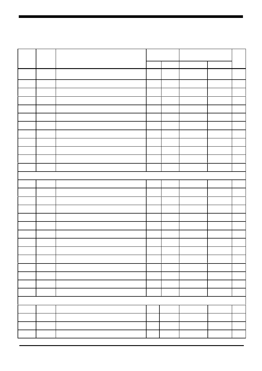
Electrical Characteristics (AC)
(T
a
= 0 ~ 70 or -40 ~ 85, V
CC
= 5V ± 20%, V
SS
=0V)
12MHz CLOCK
VARIABLE
CLOCK
SYSBOL FIGURE
PARAMETER
MIN
MAX
MIN
MAX
UNIT
1/t
CLCL
Oscillator frequency : Speed Versions
60C32/60C52
3.5
16
MHz
t
LHLL
1
ALE pulse width
127
2t
CLCL
-40
t
AVLL
1
Address valid to ALE low
43
t
CLCL
-40
t
LLAX
1
Address hold after ALE low
53
t
CLCL
-30
t
LLIV
1
ALE low to valid instruction in
234
4t
CLCL
-100
t
LLPL
1
ALE low to PSEN low
53
t
CLCL
-30
t
PLPH
1
PSEN pulse with
205
3t
CLCL
-45
t
PLIV
1
PSEN low to valid instruction in
145
3
CLCL
-105
t
PXIX
1
Input instruction hold after PSEN
0
0
t
PXIZ
1
Input instruction float after PSEN
59
t
CLCL
-25
t
AVIV
1
Address to valid instruction in
312
5t
CLCL
-105
t
PLAZ
1
PSEN low to address float
10
10
Data Memory
t
RLRH
2, 3
RD pulse width
400
6t
CLCL
-100
t
WLWH
2, 3
WR pulse width
400
6t
CLCL
-100
t
RLDV
2, 3
RD low to valid data in
252
5t
CLCL
-165
t
RHDX
2, 3
Data hold after RD
0
0
t
RHDZ
2, 3
Data float after RD
107
2t
CLCL
-70
t
LLDV
2, 3
ALE low to valid data in
517
8t
CLCL
-150
t
AVDV
2, 3
Address to valid data in
585
9t
CLCL
-165
t
LLWL
2, 3
ALE low to RD or WR low
200
300
3t
CLCL
-50 3t
CLCL
+50
t
AVWL
2, 3
Address valid to WR low or RD low
203
4t
CLCL
-130
t
QVWX
2, 3
Data valid to WR transition
33
t
CLCL
-50
t
WHQX
2, 3
Data hold after WR
33
t
CLCL
-50
t
QVWH
2, 3
Data valid to WR High
433
7t
CLCL
-150
t
RLAZ
2, 3
RD low to address float
0
0
t
WHLH
2, 3
RD or WR high to ALE high
43
123
t
CLCL
-40
t
CLCL
-40
External Clock
t
CHCX
4
High time
20
20
t
CLCX
4
Low time
20
20
t
CLCH
4
Rise time
20
20
t
CHCL
4
Fall time
20
20
SD60C32/P SD60C52/P
KSI-W015-000
9
Electrical Characteristics (Continued)
(T
a
= 0 ~ 70 or -40 ~ 85, V
CC
= 5V ± 20%, V
SS
=0V)
16MHz
CLOCK
VARIABLE CLOCK
SYMB
OL
FIGUR
E
PARAMETER
MIN MAX
MIN
MAX
UNI
T
1/t
CLCL
Oscillator frequency : Speed Versions
60C52/60C32
3.5
16
MHz
t
LHLL
1
ALE pulse width
85
2t
CLCL
-40
t
AVLL
1
Address valid to ALE low
23
t
CLCL
-40
t
LLAX
1
Address hold after ALE low
33
t
CLCL
-30
t
LLIV
1
ALE low to valid instruction in
150
4t
CLCL
-100
t
LLPL
1
ALE low to PSEN low
23
t
CLCL
-40
t
PLPH
1
PSEN pulse with
143
3t
CLCL
-45
t
PLIV
1
PSEN low to valid instruction in
83
3
CLCL
-105
t
PXIX
1
Input instruction hold after PSEN
0
0
t
PXIZ
1
Input instruction float after PSEN
38
t
CLCL
-25
t
AVTV
1
Address to valid instruction in
208
5t
CLCL
-105
t
PLAZ
1
PSEN low to address float
10
10
Data Memory
t
RLRH
2, 3
RD pulse width
275
6t
CLCL
-100
t
WLWH
2, 3
WR pulse width
275
6t
CLCL
-100
t
RLDV
2, 3
RD low to valid data in
148
5t
CLCL
-165
t
RHDX
2, 3
Data hold after RD
0
0
t
RHDZ
2, 3
Data float after RD
55
2t
CLCL
-70
t
LLDV
2, 3
ALE low to valid data in
350
8t
CLCL
-150
t
AVDV
2, 3
Address to valid data in
398
9t
CLCL
-165
t
LLWL
2, 3
ALE low to RD or WR low
138
238
3t
CLCL
-50
3t
CLCL
+50
t
AVWL
2, 3
Address valid to WR low or RD low
120
4t
CLCL
-130
t
ZVWX
2, 3
Data valid to WR transition
13
t
CLCL
-50
t
WHQX
2, 3
Data hold after WR
13
t
CLCL
-50
t
QVWH
2, 3
Data valid to WR High
288
7t
CLCL
-150
t
RLAZ
2, 3
RD low to address float
0
0
t
WHLH
2, 3
RD or WR high to ALE high
23
103
t
CLCL
-40
t
CLCL
+40
External Clock
t
CHCX
4
High time
20
20
t
CLCX
4
Low time
20
20
t
CLCH
4
Rise time
20
20
t
CHCL
4
Fall time
20
20
SD60C32/P SD60C52/P
KSI-W015-000
10
Timing Diagram
SD60C32/P SD60C52/P
ALE
PSEN
PORT0
PORT2
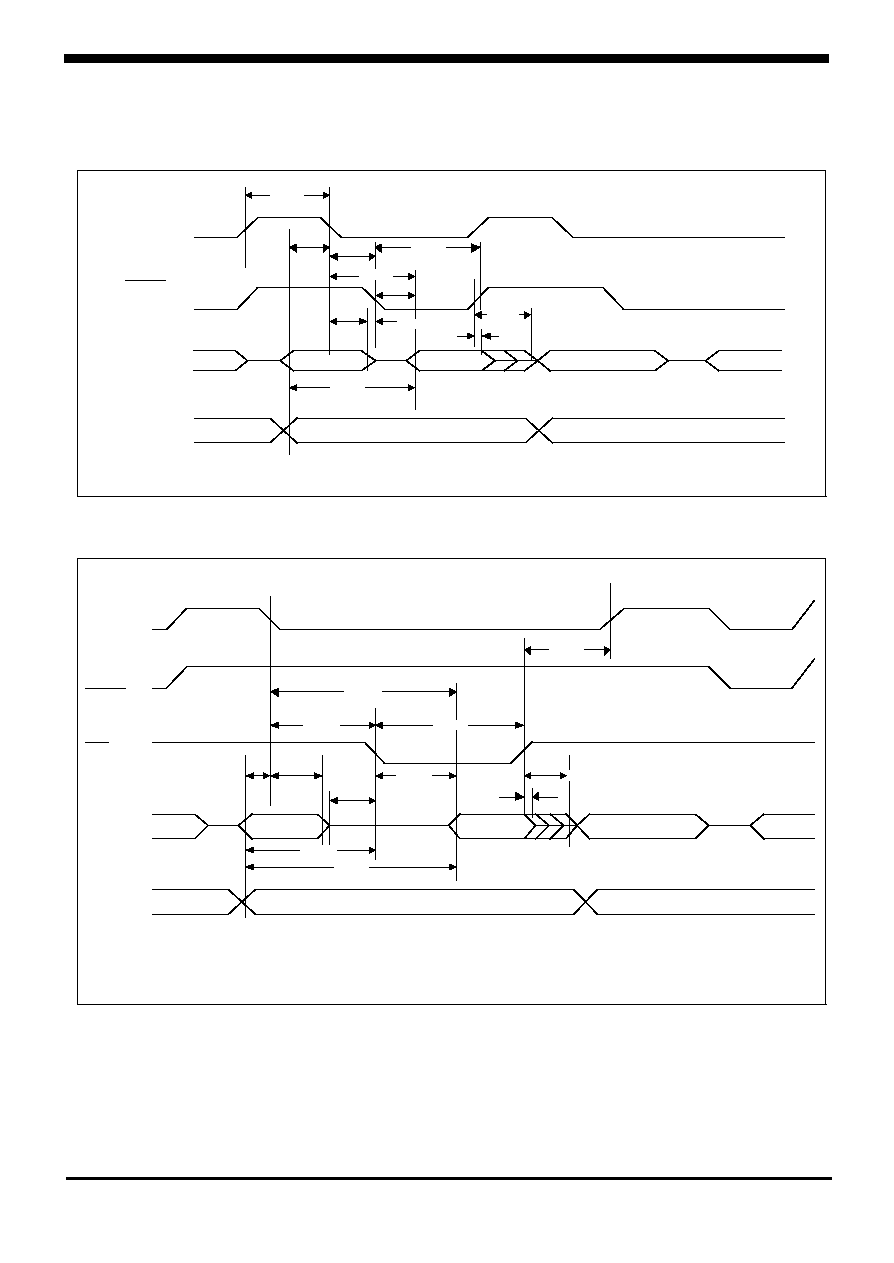
F i g u r e 2 . E x t e r n a l D a t a M e m o r y R e a d C y c l e
RD
A0 - A7
FROM RI OR DPL
DATA IN
A0 - A7 FROM PCL
INSTR IN
P2.0 - P2.7 OR A8 - A15 FROM DPH
A0 - A15 FROM PCH
t
WHLH
t
LLDV
t
LLWL
t
RLRH
t
RHDZ
t
RHDX
t
RLDV
t
RLAX
t
L L A X
t
AVLL
t
AVWL
t
AVDV
t
LHLL
ALE
PSEN
PORT0
PORT2
t
A V L L
t
LLPL
t
LLIV
t
PLIV
t
L L A X
t
PLAZ
t
PXIX
t
PXIZ
t
AVIV
A0 - A7
INSTR IN
A0 - A7
A8 - A15
A0 - A15
F i g u r e 1 . E x t e r n a l P r o g r a m M e m o r y R e a d C y c l e
t
PLPH
KSI-W015-000
11
Timing Diagram (Continued)
SD60C32/P SD60C52/P
t
QVWX
ALE
PSEN
PORT0
PORT2
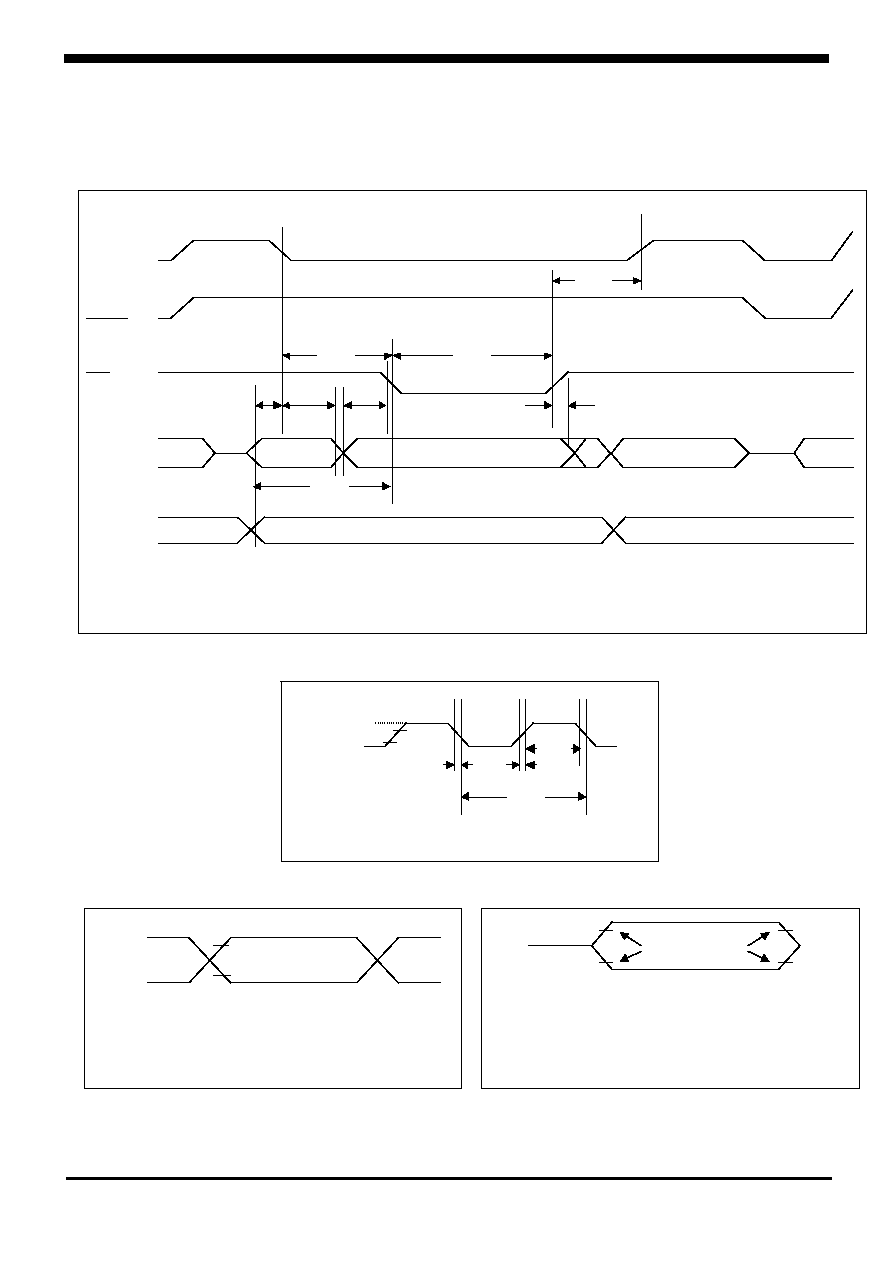
F i g u r e 3 . E x t e r n a l D a t a M e m o r y W r i t e C y c l e
WR
P2.0 - P2.7 OR A8 - A15 FROM DPH
A0 - A15 FROM PCH
t
WHLH
t
LLWL
t
WLWH
t
WHQX
t
LLAX
t
AVLL
t
AVWL
A0 - A7 FROM PCL
INSTR IN
DATA OUT
A0 - A7
FROM RI OR DPL
V
CC
- 0.5
0.45V
0.7V
CC
0.2V
SS
-0.1
t
CLCL
t
CLCX
t
CHCX
t
CLCH
t
CHCL
F i g u r e 4 . E x t e r n a l C l o c k D r i v e
F i g u r e 5 . A C T e s t i n g I n p u t / O u t p u t
0.2V
CC
+0.9
0.2V
CC
-0.1
V
CC
-0.5
0.45V
NOTE :
AC Inputs during testing are driven at V
CC
-0.5 for a logic
'1' and 0.45V for a logic '0'. Timing measurements are
made at V
IH
min for a logic '1' and V
IL
for a logic '0'
Figure 6. Float Waveform
NOTE :
For timing purposes, a port is no longer floating when a
100mV change from load voltage occurs, and begings
to float when a 100mV change from the loaded V
OH
/V
OL
level occurs. I
OH
/I
OL
20mA
TIMING
REFERENCE
POINTS
V
LOAD
V
LOAD
- 0.1V
V
LOAD+
+ 0.1V
V
OL
+ 0.1V
V
OH
- 0.1V
KSI-W015-000
12
Timing Diagram (Continued)
SD60C32/P SD60C52/P
V
CC
I
CC
(NC)
V
CC
P0
EA
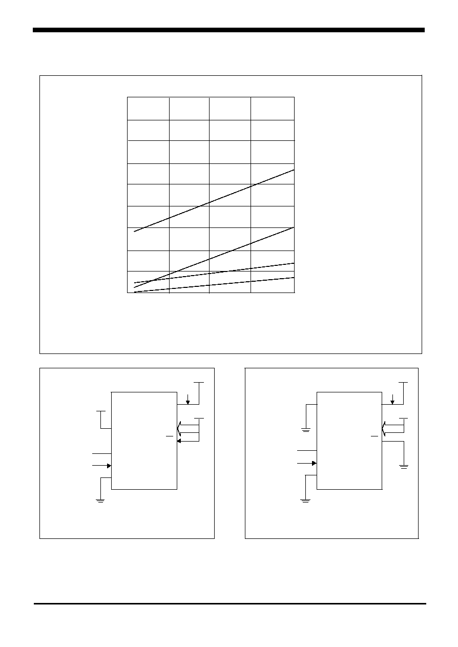
CLOCK SIGNAL
XTAL2
XTAL1
V
SS
Figure 9. I
C C
Test Condition, Idle Mode
All other pins are disconnected
RST
V
CC
V
CC
I
CC
(NC)
V
CC
P0
EA
V
CC
CLOCK SIGNAL
XTAL2
XTAL1
V
SS
Figure 8. I
C C
Test Condition, Active Mode
All other pins are disconnected
RST
I
CC
4MHz
8MHz
12MHz
45
40
35
30
25
20
15
10
5
16MHz
TYP IDLE MODE
MAX IDLE MODE
TYP ACTIVE MODE
MAX ACTIVE MODE
FREQ AT XTAL1
F i g u r e 7 .
Icc
v s . F R E Q
Valid only within frequency specifications
of the device under test
KSI-W015-000
13
Timing Diagram (Continued)
SD60C32/P SD60C52/P
V
CC
- 0.5
0.45V
0.7V
CC
0.2V
SS
- 0.1
t
CLCL
t
CLCX
t
CHCX
t
CLCH
t
CHCL
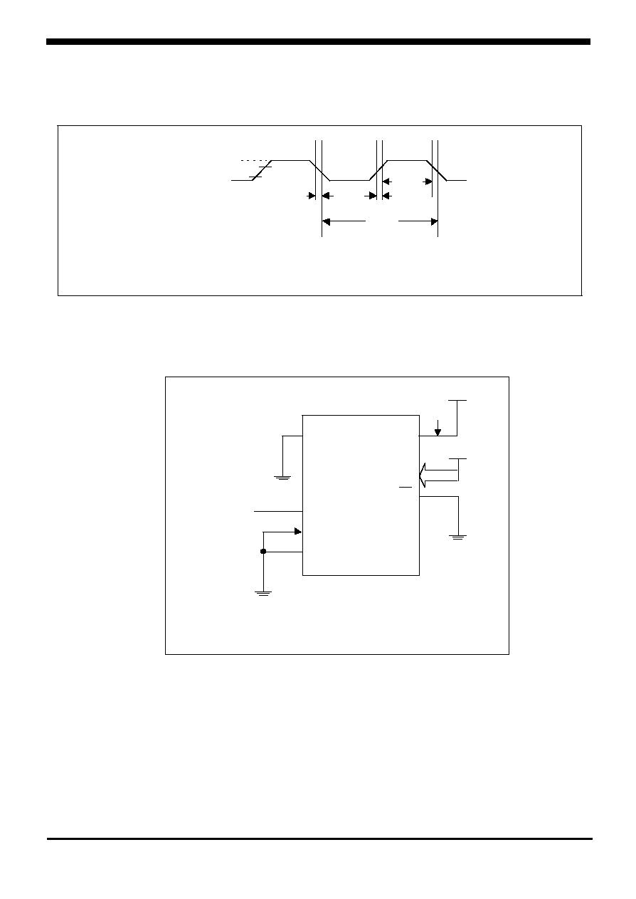
F i g u r e 1 0 . C l o c k S i g n a l W a v e f o r m f o r I T e s t s i n A c t i v e a n d I d l e M o d e s
t
C L C H
= t
C H C L
= 5
V
CC
I
CC
(NC)
V
CC
P0
EA
XTAL2
XTAL1
V
SS
F i g u r e 1 1 . I T e s t C o n d i t i o n , P o w e r d o w n M o d e
A l l o t h e r p i n s a r e d i s c o n n e c t e d , V = 2 V t o 5 . 5 V
RST
V
CC
c c
c c
c c