KSD-3004-000
1
SDS142WK
Switching Diode
Features
∑
∑
∑
∑
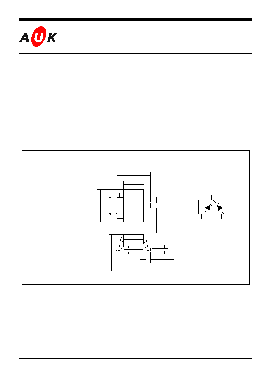
SMD package : SOT-323
∑
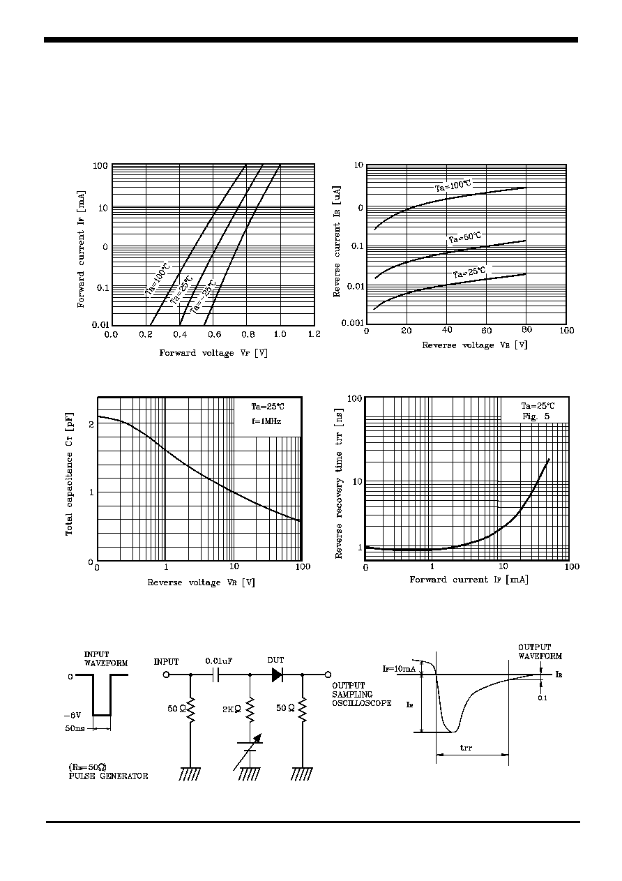
Low forward voltage : V
F
=0.9V(Typ.)
∑
Fast reverse recovery time : t
rr
=1.6ns(Typ.)
∑
Small total capacitance : C
T
=2.2pF(Typ.)
∑
Ultra high speed
Ordering
Information
Type No.
Marking
Package Code
SDS142WK
A6
SOT-323
Outline Dimensions unit :
mm
PIN Connections
1. Anode
2. Anode
3. Cathode, Cathode
1
3
S
S
e
e
m
m
i
i
c
c
o
o
n
n
d
d
u
u
c
c
t
t
o
o
r
r
2
2.1
±
0.1
1.25
±
0.05
1
2.
0
±
0.
2
0.
3
0
±
0.
1
2
0.1 Min.
1.
3
0
±
0.
1
0.
9
0
±
0.
1
0.
1
5
±
0.
05
3
0~
0.
1
KSD-3004-000
2
SDS142WK
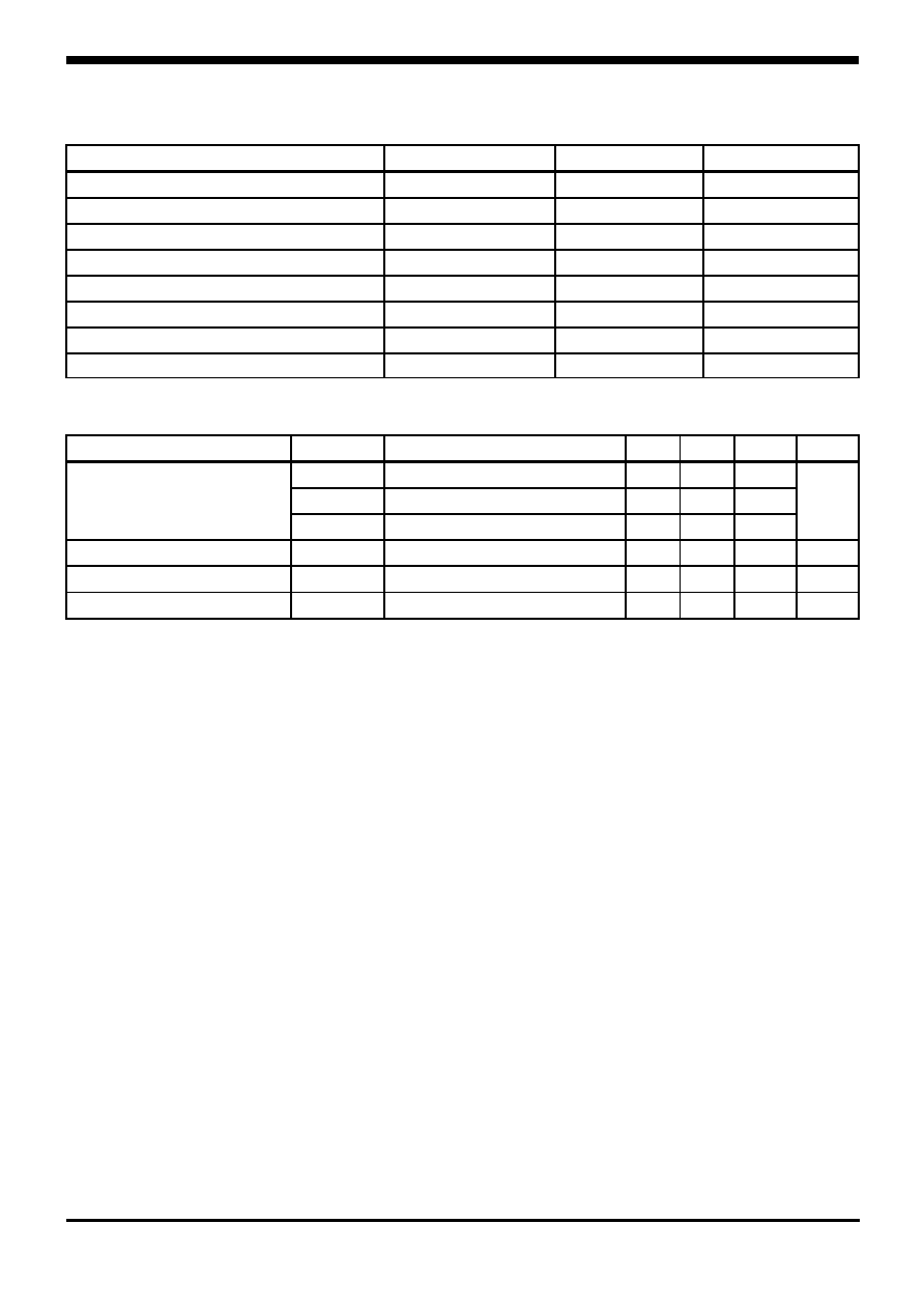
Absolute maximum ratings
Ta=25
∞
C
Characteristic
Symbol
Ratings
Unit
Maximum(peak) reverse voltage
V
RM
85
V
Reverse voltage
V
R
80
V
Maximum(peak) forward current
I
FM
*
300
mA
Average forward current
I
O
*
100
mA
Surge current(10ms)
I
FSM
*
2
A
Power dissipation
P
D
150
mW
Junction temperature
T
j
150
∞
C
Storage temperature
T
stg
-55 ~ 150
∞
C
* : Unit ratings. Total rating = Unit rating
◊
1.5
Electrical Characteristics
Ta=25
∞
∞
∞
∞
C
Characteristic
Symbol
Test Condition
Min. Typ. Max.
Unit
V
F(1)
I
F
=1mA
-
0.6
-
V
F(2)
I
F
=10mA
-
0.7
-
Forward voltage
V
F(3)
I
F
=100mA
-
0.9
1.2
V
Reverse current
I
R
V
R
=80V
-
-
0.5
µ
A
Total capacitance
C
T
V
R
=0, f=1MHz
-
2.2
4.0
pF
Reverse recovery time
t
rr
I
F
=10mA
-
1.6
4.0
ns