Äîêóìåíòàöèÿ è îïèñàíèÿ www.docs.chipfind.ru
KSD-O3D013-000
1
SHE144PGIE(B)
Oval Type High Efficiency LED Lamp
Features
· Green colored transparency lens type
· Ellipse type(X=4.6mm, Y=5.8mm)
· Ultra luminosity
· Flangeless package
· High power LEDs
· Oval shape
· View Angle : 70° / 34°
· E ; ESD Protected (±2.0KV, 3 times @100pF, 1.5K)
Application
· Full color displays
· Message boards
· Variable message signs(VMS)
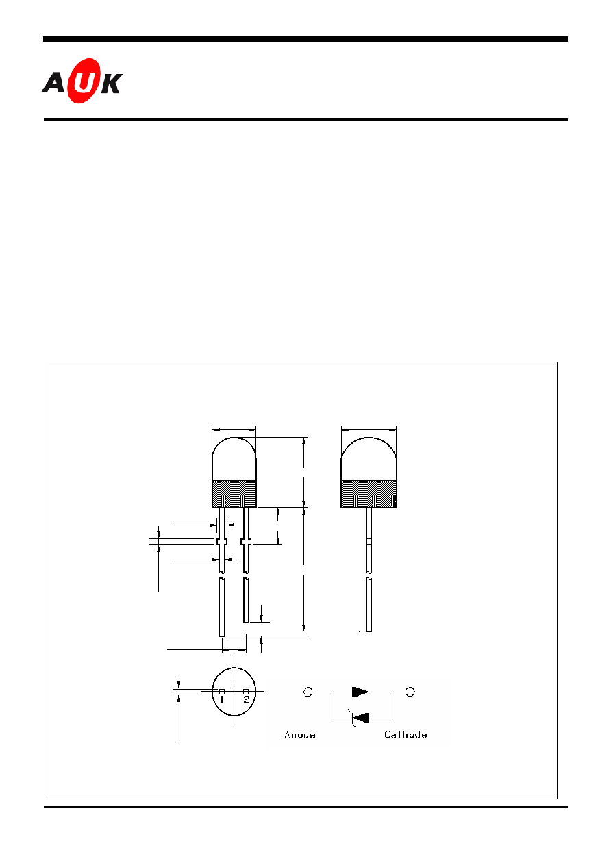
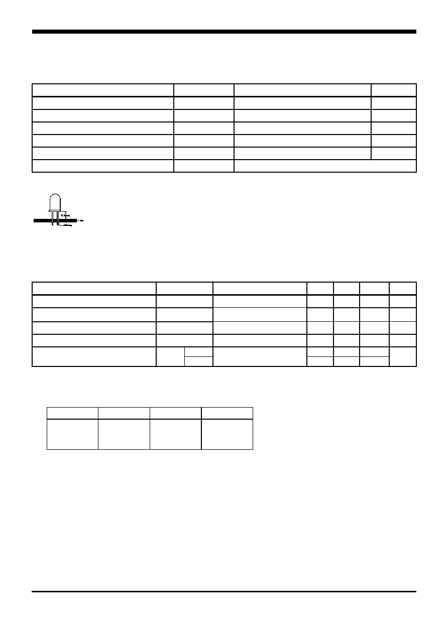
Outline Dimensions unit :
mm
S
S
e
e
m
m
i
i
c
c
o
o
n
n
d
d
u
u
c
c
t
t
o
o
r
r
4 . 4 0 ~ 4 . 8 0
5.50~6.00
7 . 5 0 ~ 7 . 9 0
3.10~4.10
1.20 Min.
0.55 Max.
1
.
2
7
T
y
p
.
22.00 Min.
1.00 Min.
2.54 Typ.
0
.
5
5
M
a
x
.
PIN Connections
1. Anode
2. Cathode
KSD-O3D013-000
2
SHE144PGIE(B)
Absolute Maximum Ratings
(Ta=25
o
C)
Characteristic Symbol
Rating
Unit
Power dissipation
P
D
150
mW
Forward current
I
F
40
mA
*
1
Peak forward current
I
FP
65
mA
Operating temperature range
T
opr
-30 85
Storage temperature range
T
stg
-30 100
*
2
Soldering temperature
T
sol
260
for
10 seconds
*1.Duty ratio = 1/16, Pulse width = 0.1ms
*2.Keep the distance more than 2.0mm from PCB to the bottom of LED package
Recommend document
-. LED is very sensitive to ESD.
Electrical / Optical Characteristics
(Ta=25
o
C)
Characteristic Symbol
Test
Condition
Min.
Typ.
Max.
Unit
Forward voltage
V
F
I
F
= 20mA
-
3.2
3.8
V
*
4
Luminous intensity
I
V
I
F
= 20mA
1760
-
5940
mcd
Dominant wavelength
D
I
F
= 20mA
515
522
530
nm
Spectrum bandwidth
I
F
= 20mA
-
30
-
nm
X
-
±17
-
*
3
Half angle
1/2
Y
I
F
= 20mA
-
±35
-
deg
*3.
1/2
is the off-axis angle where the luminous intensity is
1/2
the peak intensity
*4. Luminous intensity maximum tolerance for each grade classification limit is ±18%
*4. Luminous Intensity Classification
S T
1
T
2
U
1760~2640 2640~3300 3300~3960 3960~5940
(Do not use to combine grade classification. It must be used separately grade classification)
KSD-O3D013-000
3
SHE144PGIE(B)
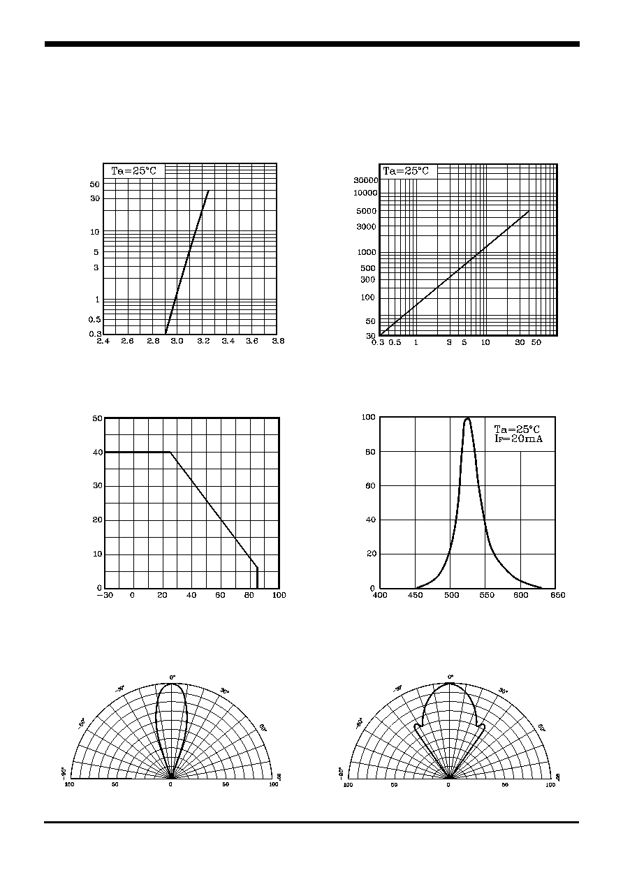
Characteristic Diagrams
Fig. 1 I
F
- V
F
Fig.4 Spectrum Distribution
Fig. 3 I
F
Ta
Fig. 2 I
V
- I
F
F
o
rward Current
I
F
[mA]
Ambient Temperature Ta []
R
e
lative Int
e
nsit
y
[%]
Wavelength [nm]
Forward Voltage V
F
[V]
F
o
rward Current
I
F
[mA]
Forward Current I
F
[mA]
Luminous Intensit
y I
v
[mc
d
]
Relative Luminous Intensity Iv [%]
Fig. 5-1 Radiation Diagram(X)
Fig. 5-2 Radiation Diagram(Y)
Relative Luminous Intensity Iv [%]
KSD-O3D013-000
4
1. ESD(Electro Static Discharge) : Chip Al
2
o
3
(Sapphire: )
Chip Damage
V
F
Down
2. ESD
2-1. ESD (Electro Static Discharge) :
(+) (-)
( , , , )
(-) (+)
(+) (-) .
: , , , , ,
: , , , ,
: , .
2-2.
-.
.
80% .
-.
-. :
Wrist Strap ( ), Heel Grounder, , , ,
-. Conveyer Table
: Conductive Floor Mat
ESD
.
(10%~20%) (65%~90%)
Table
6[KV]
0.1[KV]
7[KV]
0.6[KV]
20[KV]
1.2[KV]

KSD-O3D013-000
5
SHE144PGIE(B)
The AUK Corp. products are intended for the use as components in general electronic
equipment (Office and communication equipment, measuring equipment, home
appliance, etc.).
Please make sure that you consult with us before you use these AUK Corp. products
in equipments which require high quality and / or reliability, and in equipments which
could have major impact to the welfare of human life(atomic energy control, airplane,
spaceship, transportation, combustion control, all types of safety device, etc.). AUK
Corp. cannot accept liability to any damage which may occur in case these AUK Corp.
products were used in the mentioned equipments without prior consultation with AUK
Corp..
Specifications mentioned in this publication are subject to change without notice.