 | –≠–ª–µ–∫—Ç—Ä–æ–Ω–Ω—ã–π –∫–æ–º–ø–æ–Ω–µ–Ω—Ç: SL432A | –°–∫–∞—á–∞—Ç—å:  PDF PDF  ZIP ZIP |
KSD-I0A001-002
1
SL432x
Programmable Voltage Reference
Description
The SL432 series are 3-terminal precision shunt regulators that are programmable over a wide voltage range of
1.24V to 16V with ±0.5%, ±1.0%, ±2.0% tolerance. The SL432 series have a low dynamic impedance of 0.25.
These features make the SL432 series an excellent replacement for zener diodes in numerous applications circuits
that require a precision reference voltage.
Features
∑ Programmable output voltage from 1.24V to 16V
∑ Voltage reference tolerance : ±0.5%, ±1.0%, ±2.0%
∑ Cathode current capability of 80 to 30mA
Ordering
Information
Type NO.
Marking
Package Code
SL432x
SL432
TO-92
: Grade => None:±2% , A:±1% , B:±0.5%
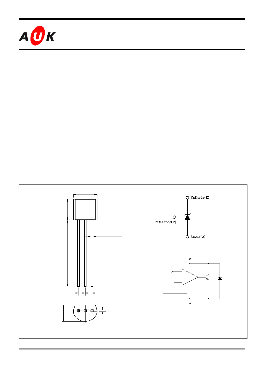
Outline Dimensions
( Unit : mm )
S
S
e
e
m
m
i
i
c
c
o
o
n
n
d
d
u
u
c
c
t
t
o
o
r
r
Symbol
Functional block diagram
PIN Connections
1. Reference
2. Anode
3. Cathode
REF
Reference(R)
+
-
V
Cathode(K)
Anode(A)
=1.24V
4.
40~4.
80
4.40~4.80
0.50 Max.
13.
50~14.
50
3.
40~3.
60
0.
45 Max.
1.27 Typ.
1.27 Typ.
1 2 3
KSD-I0A001-002
2
SL432x
Absolute maximum ratings
[Ta=25]
Characteristic
Symbol Rating
Unit
Cathode to Anode voltage
V
KA
18 V
Cathode current
I
K
30
mA
Reference input current
I
ref
3
mA
Power Dissipation
P
D
625
mW
Junction Temperature
T
J
150
Operating temperature range
T
opr
-40 ~ +85
Storage temperature range
T
stg
-55 ~ +150
Recommended operating conditions
Rating
Characteristic Symbol
Min. Max.
Unit
Cathode to Anode voltage
V
KA
V
ref
16 V
Cathode current
I
K
0.1
25
mA
Electrical Characteristics
(Ta=25 , unless otherwise noted.)
Characteristic Symbol
Condition
Min.
Typ.
Max.
Unit
SL432B 1.234
1.246
SL432A 1.228
1.252
Reference voltage (Fig.1)
V
ref
V
KA
=V
ref
, I
K
=10mA
SL432 1.215
1.240
1.265
V
Reference input voltage
deviation over temperature
(Fig.1, Note1,2)
V
ref
V
KA
=V
ref
, I
K
=10mA
@ -40∞C Ta 85∞C
- 10 20 mV
V
ref
V
ref
=V
ref (16V)
-V
ref
Ratio of delta reference input
voltage to delta cathode
voltage (Fig.2)
V
KA
I
K
=10mA
Vref V
KA
16V
V
KA
=V
KA(16V)
-V
ref
- -1.0 -2.7
mV/V
Reference current (Fig.2)
I
ref
I
K
=10mA
R1=10K
, R2=
- 1.0 1.5 µ
Reference input current
deviation over temperature
(Fig.2, Note 1,2)
I
ref
I
K
=10mA
R1=10K
, R2=
@ -40∞C Ta 85∞C
- 0.04 0.08 µ
Minimum cathode current
for regulation
I
K(MIN)
V
KA
=V
ref
-
80
100
µ
Off-state cathode current
(Fig.3)
I
K(off)
V
KA
=16V, V
ref
=0V -
5
50
nA
Dynamic impedance
(Fig.1, Note3)
Z
KA
V
KA
=V
ref
, f
1.0KHz
0.1mA I
K
25mA
- 0.25 0.4
KSD-I0A001-002
3
SL432x
1
ref
2
1
ref
KA
R
◊
I
+
)
R
R
+
1
(
◊
V
=
V
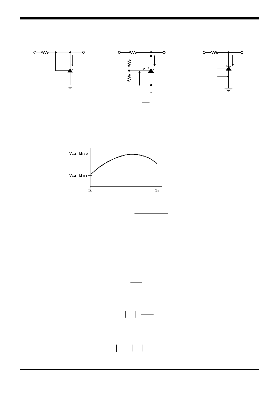
Note.
1. Ambient temperature range: T
LOW
= -40, T
High
= 85
2. The deviation parameters V
ref
and I
ref
are defined as the difference between the maximum value and minimum value
obtained over the full operating ambient temperature range that applied.
The average temperature coefficient of the reference input voltage,
ref
V
is defined as:
T
)
10
◊
)
25
=
T
(
V
V
(
=
)
ppm
(
V
a
6
a
ref
ref
ref
ref
V
can be positive or negative depending on whether V
ref
Min or V
ref
Max occurs at the lower ambient temperature, refer to
Fig. 8
Example : V
ref
= 10mV and the slope is positive,
V
ref
@ 25 = 1.24V
T
a
= 125
/
ppm
65
=
125
10
◊
)
241
.
1
010
.
0
(
=
)
ppm
(
V
6
ref
3. The dynamic impedance Z
KA
is defined as:
K
KA
KA
I
V
=
When the device is operating with two external resistors, R1 and R2, (refer to Fig.2) the total dynamic impedance of the circuit
is given by:
)
R
R
+
1
(
◊
=
2
1
KA
'
KA
Fig. 1 Test circuit for V
KA
=V
ref
Fig. 2 Test circuit for V
KA
>V
ref
Fig. 3 Test circuit for I
K(off)
V
ref
= V
ref
Max ≠ V
ref
Min
T
a
= T
2
≠ T
1
Ambient Temperature
KA
Input
R1
R2
V
V
KA
Input
I
K(off)
I
ref
V
ref
I
K
KA
V
Input
I
K
KSD-I0A001-002
4
SL432x
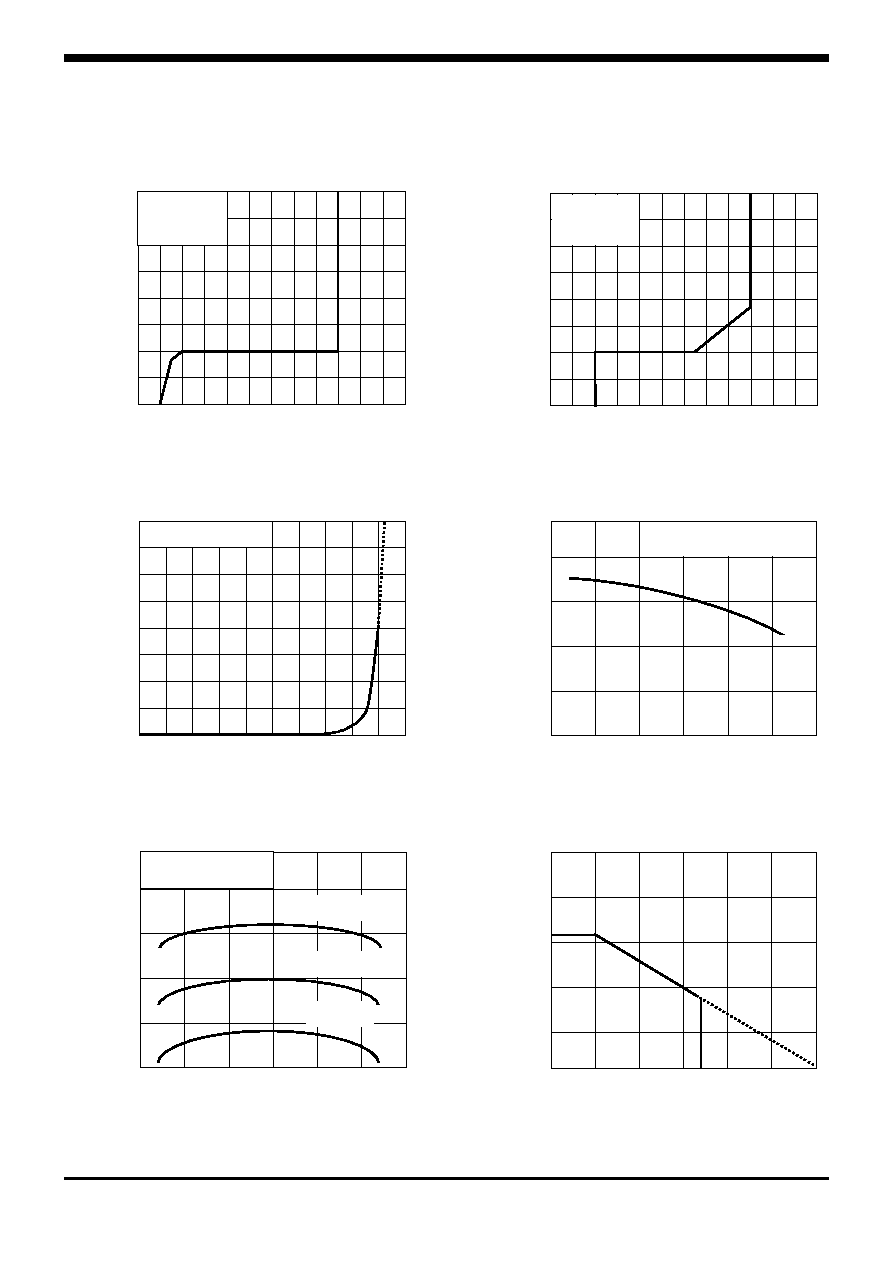
Electrical Characteristics Curves
(Continue)
Cathode Voltage V
KA
[V]
0.0
20
0.1
0.3
0.2
0
16
8
0.4
Of
f-state cathode c
u
rrent
I
K(of
f)
[µ
A
]
12
4
V
ref
=0V, Ta=25∞C
2.0
Cath
od
e
cu
rr
e
n
t I
KA
[
µA]
0
0
0.5
1.0
300
50
-0.5
-1
1.5
250
200
-
50
150
100
-10
Fig.4 I
K
vs V
KA
(1)
Fig.5 I
K
vs V
KA
(2)
Fig.6 I
K(off)
vs V
KA
I
20
1.5
10
-
10
1.0
Cathode c
u
rrent I
K
[mA]
0
Cathode Voltage V
KA
[V]
2.0
0.5
-0.5
-1
0
30
V
KA
=V
ref
Ta=25∞C
Cathode Voltage V
KA
[V]
V
KA
=V
ref
Ta=25∞C
Fig.8 V
ref
vs T
a
50
0
1.30
-25
1.26
75
25
100
1.28
1.22
1.24
1.20
-50
Ref
e
r
e
n
ce input v
o
ltag
e
V
ref
[V
]
Ambient Temperature T
a
[∞C]
V
KA
=V
ref ,
I
K
=10mA
V
ref(min)
V
ref(typ)
V
ref(max)
Fig.7 V
ref
/V
KA
vs T
a
50
0
0.0
-25
-0.2
75
25
100
-0.1
-0.4
-0.3
-0.5
-50
Ratio o
f
de
lta
ref
e
renc
e inpu
t vo
lt
age
to d
e
lt
a
cathod
e voltage
V
ref
/
V
KA
[mV/V]
Ambient Temperature T
a
[∞C]
V
ref
V
KA
16V, I
K
=10mA
Fig.9 P
D
vs T
a
Ambient Temperature T
a
[∞C]
100
50
25
125
75
150
0
Po
wer
di
ssi
pat
i
o
n
P
D
[m
W]
0
1000
600
800
200
400
KSD-I0A001-002
5
SL432x
Electrical Characteristics Curves
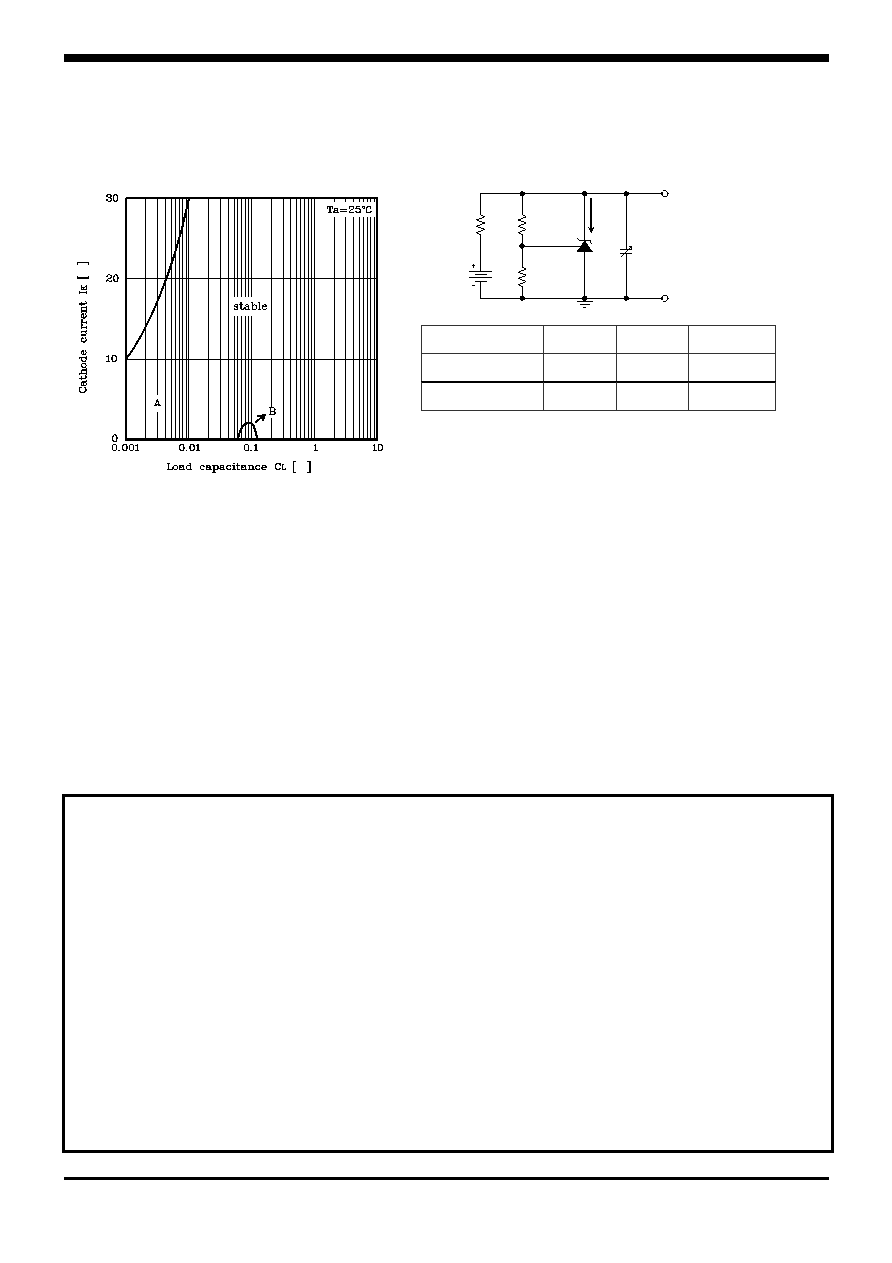
Unstable Regions
V
KA
R
1
[K] R
2
[K]
A, B
V
ref
0
A 10V
10
1.415
R2
CL
0
GND
R1
Output
The AUK Corp. products are intended for the use as components in general electronic
equipment (Office and communication equipment, measuring equipment, home
appliance, etc.).
Please make sure that you consult with us before you use these AUK Corp. products
in equipments which require high quality and / or reliability, and in equipments which
could have major impact to the welfare of human life(atomic energy control, airplane,
spaceship, transportation, combustion control, all types of safety device, etc.). AUK
Corp. cannot accept liability to any damage which may occur in case these AUK Corp.
products were used in the mentioned equipments without prior consultation with AUK
Corp..
Specifications mentioned in this publication are subject to change without notice.
Fig.10 Stability Boundary Conditions
I
K
Fig.11 Test circuit for Fig. 10