 | –≠–ª–µ–∫—Ç—Ä–æ–Ω–Ω—ã–π –∫–æ–º–ø–æ–Ω–µ–Ω—Ç: SL5015 | –°–∫–∞—á–∞—Ç—å:  PDF PDF  ZIP ZIP |
KSI-W003-000
1
SL5015/P
COMPANDOR
Description
The SL5015/P is an noise reduction IC for cordless phone. It is a compandor IC that consist
of a compressor and an expander. Compandor reduces transmission noise by compressing
and transmitting out going signals and expanding received signals.
The ICs are designed for minimum requirement of external components and for low voltage
operation. Small size is an advantage when used in equipment in which space is a premium.
For DATA, input and output terminals are provided for convenience. Two styles of packaging,
DIP and SOP, are available to meet different requirements.
Features
∑
Low voltage operation V
opr
. = 2.4~7.0V
∑
Low current consumption I
CC
= 4mA(Vcc=3V)
∑
Microphone amplifier used in compressor
∑
Has data input output terminals
∑
Has a buffer amplifier for filter
∑
Mute can be set up independently
∑
Through Functions
∑
Built in limiter (for compressor)
Ordering
Information
Type NO.
Marking
Package Code
SL5015
SL5015
SOP20
SL5015P
SL5015
DIP20
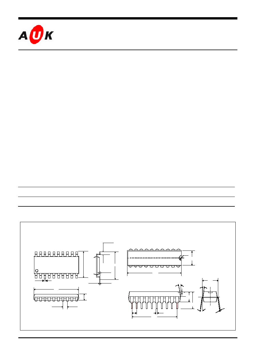
Outline Dimensions unit :
mm
2.54
0.46
3.30
1.52
0.51
7.11
22.84
7
o
5
o
-7
o
0.25
7
o
7.62
26.14
0.89R
7.62
1
10
20
11
S
S
e
e
m
m
i
i
c
c
o
o
n
n
d
d
u
u
c
c
t
t
o
o
r
r
0.25
0.22
0.58
10.31
12.83
1.27
2.56
7.52
0.41
SOP20
DIP20
KSI-W003-000
2
Absolute Maximum Ratings
(Ta = 25
∞
C)
Characteristics
Symbol
Rating
Unit
Maximum Supply Voltage
V
CC
10
V
1000(D) note 1
mW
Power Dissipations
P
D
410(S) note 2
Operating Temperature Range
T
opr
-20 ~ 70
∞C
Storage Temperature Range
T
stg
-55 ~ 150
∞C
*
note 1. Above Ta=+25 ∞C , derate at 8mW/∞C
2. Above Ta=+25 ∞C, derate at 3.3mW/∞C
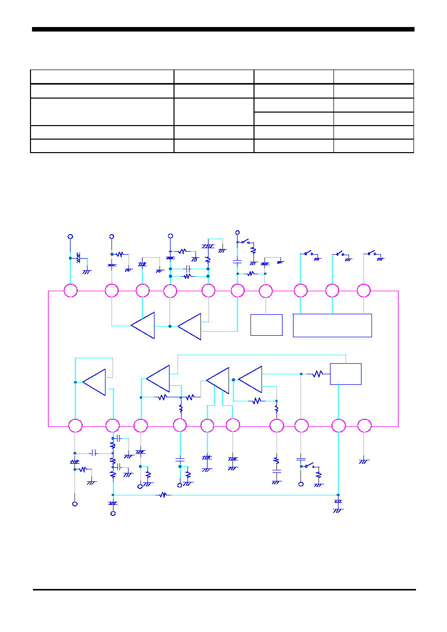
Block Diagram and Test Circuit
SL5015/P
2.2
20
19
18
17
16
15
14
13
12
11
1
2
3
4
5
6
7
8
9
10
R E G .
L O G I C M U T E
-
+
-
+
-
+
E X P .
C O M
-
+
R E G .
1 0 0 K
1 0 0 K
1 0 0 K
5 1 K
3 . 3 K
1 0 0 K
1 0
1 0 K
1
2.2
2.2
1 0 K
5 0 p F
5 1 K
1 0 K
1
0.047
1 0 0 K
6 0 0
4.7
V c c
E X P . O U T
D A T A O U T
E X P . I N
S W 2
S W 3
S W 4
S W 5
E X P .
M U T E
T H R O U G H
C O M P .
M U T E
+
+
+
+
+
+
+
+
+
+
+
+
4.7
6 0 0
S W 1
0.047
C O M P . I N
0 . 4 7
9 . 1 K
2.2
R E C T
D C F
6 0 0
0.1
1 0 0 K
D A T A I N
C O M P . O U T
1
1 0 K
6 0 0 0 p F
1 0 K
1 0 K
1 0 K
1 0 K
1 0 0 0 p F
1 8 0 0 p F
1 u F
F I L T E R O U T
F I L T E R I N
KSI-W003-000
3
Switch Position
Switch terminal
High (Open or Vcc)
Low(GND)
PIN 11(SW3)
Comp Mute OFF
Comp Mute ON
PIN 12(SW4)
Compandor
Through
PIN 13(SW5)
Exp Mute OFF
Exp Mute ON
PIN 8 (SW1)
Signal Input OFF
PIN 15 (SW2)
Signal Input OFF
Electrical Characteristics
(Unless otherwise specified, Ta=25 ∞C, Vcc=3V, f=1kHz, RL = 10 k)
Characteristics
Symbol
Test Conditions
Min.
Typ.
Max.
Unit
Squelch Current
I
CCQ
No Signal
-
4.0
6.5
mA
Reference Voltage
V
ref
-
1.4
1.5
1.55
V
Compressor
Input Resistance
R
IN
-
90
120
-
k
Standard Input Level
V
IN
V
OUT
=300mVrms = 0dB
8.0
12.5
17.0
mV
rms
Gain error(1)
G
V
(1)
V
IN
= -20dB
-0.5
0
+0.5
dB
Gain error(2)
G
V
(2)
V
IN
= -40dB
-0.1
0
+1.0
dB
Through ON/OFF Diff.
G
V
V
IN
=0dB, 12 pin GND
-1.5
0
+1.5
dB
Distortion
THD
V
IN
= 620
-
0.5
1.0
%
Noise output
V
NO
Rg= 620
-
3.0
5.5
mV
rms
Muting attenuation
M
ATT
V
IN
= 0dB, 11 Pin GND
60
80
-
dB
Limiting voltage
V
LI
-
1.15
1.35
1.50
V
p-p
Expander
Standard Input Level
V
OUT
V
IN
= 30mVrms = 0dB
110
130
160
mV
rms
Gain error(1)
G
V
(1)
V
IN
= -10dB
-0.5
0
+0.5
dB
Gain error(2)
G
V
(2)
V
IN
= -20dB
-1.0
0
+1.0
dB
Gain error(3)
G
V
(3)
V
IN
= -30dB
-1.5
0
+1.5
dB
Through ON/OFF Diff.
G
V
V
IN
= 0dB, 12 Pin GND
-2.5
-1.0
+0.5
dB
Distortion
THD
V
IN
= 0dB
-
0.5
1.5
%
Noise output
V
NO
Rg= 620
-
10
30
V
rms
Muting attenuation
MATT
V
IN
= 0dB, 13 pin
60
80
-
dB
Max. output voltage
V
OUT(max)
THD 10% level
700
800
-
mV
rms
SL5015/P
KSI-W003-000
4
Electrical Characteristics(continued)
(Unless otherwise specified, Ta=25 ∞C, Vcc=3V, f=1kHz, RL = 10 k)
Characteristics
Symbol
Test Conditions
Min.
Typ.
Max.
Unit
Buffer Amp(LPF)
Voltage Gain
G
V
V
IN
= 300mVrms
-0.5
0
0.5
dB
Freq Charact(1)
f
1
V
IN
=300mVrms, f=3kHz
-4.5
-3
0
dB
Freq Charact(2)
f
2
V
IN
=300mVrms, f=30kHz
-75
-60
-55
dB
Distortion
THD
V
IN
= 300mVrms
-
0.02
0.1
%
(PIN VOLTAGE AT VCC=3V AND NO INPUT SIGNAL)
Pin. No.
NAME
TYPE.
VAL
Unit
Pin. No.
NAME
TYPE.
VOL
Unit
1
FILTER OUT
1.5
V
11
COMP MUTE
1.3
V
2
FILTER IN
1.5
V
12
THROUGH
1.3
V
3
COMP OUT
1.5
V
13
EXP MUTE
1.3
V
4
DATA IN
1.5
V
14
EXP REF
1.5
V
5
C-DCF
1.5
V
15
EXP IN
1.5
V
6
COMP RECT
0.6
V
16
EXP NF
1.5
V
7
COMP NF
1.5
V
17
DATA OUT
1.5
V
8
COMP IN
1.5
V
18
EXP RECT
0.6
V
9
COMP REF
1.5
V
19
EXP OUT
1.5
V
10
GND
GND
V
20
VCC
VCC
V
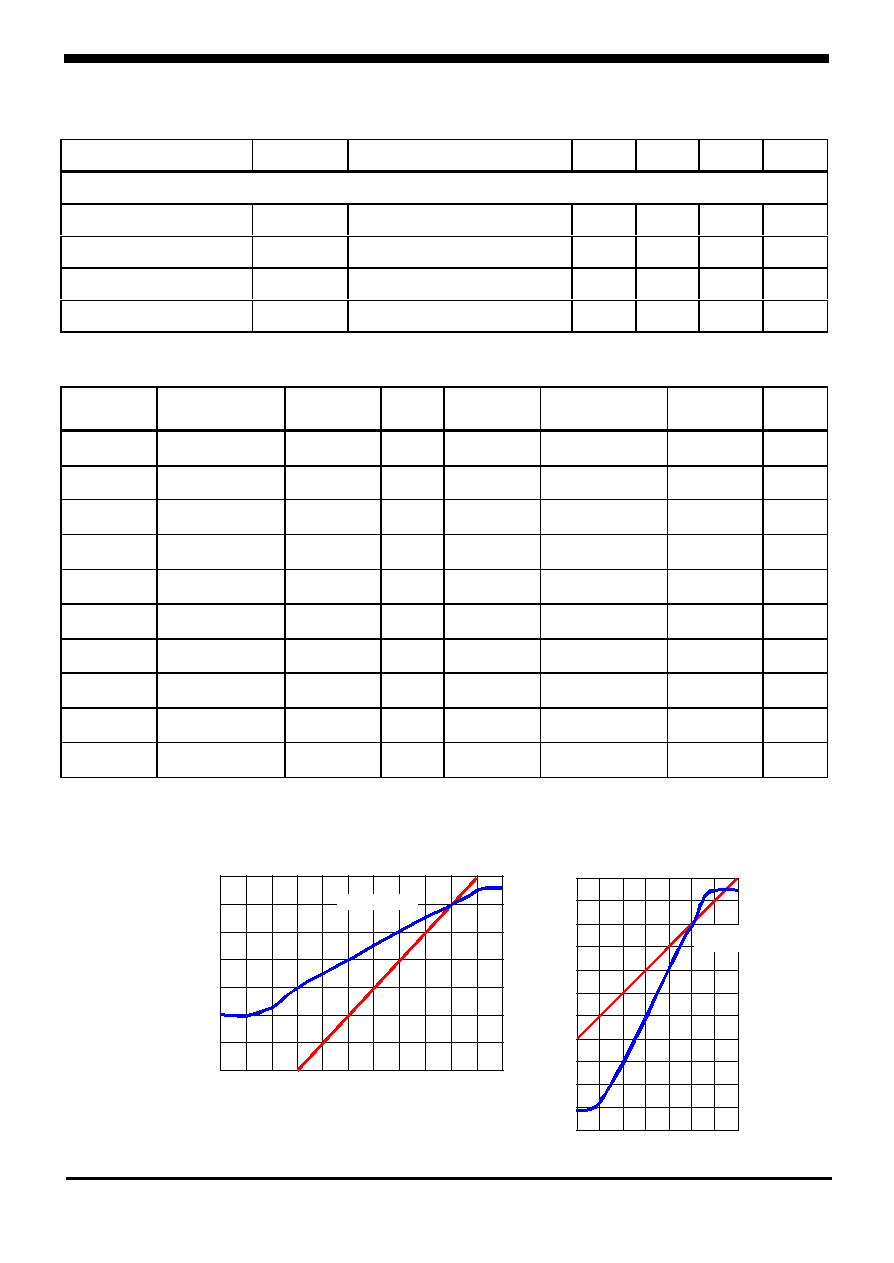
Typical Performance Characteristics
∑
Input Voltage VS Output Voltage
SL5015/P
C o m p r e s s o r
Vcc = 3.0V, Fin = 1.0KHz
-20
-130
-110
-80
-100
-90
-120
-30
-40
-50
-60
-70
-20
-10
0
-30
-40
-50
-60
-70
(300mVrms)
V i n ( d B V )
(10mVrms)
Vout(dBV)
Standard Level
E x p a n d e r
Vcc = 3.0V, Fin = 1.0KHz
-10
-20
-30
-40
-50
-60
-70
-80
0
-10
-20
-30
-40
-50
-60
-70
-80
-90
-100
-110
(100mVrms)
1.0Vrms
(30mVrms)
V i n ( d B V )
Vout(dBV)
Standard
Level