 | –≠–ª–µ–∫—Ç—Ä–æ–Ω–Ω—ã–π –∫–æ–º–ø–æ–Ω–µ–Ω—Ç: SL5022 | –°–∫–∞—á–∞—Ç—å:  PDF PDF  ZIP ZIP |
KSI-W011-000
1
SL5022/P
UNIVERSAL SPEECH NETWORK
Description
The SL5022/P can fulfill the standards of other countries by changing the external
component.
Dynamic or piezoelectric type can be used with receiver Each gain is controlled with AGC in
accordance with the line current. The SL5022/P can be operated down to DC line 1.6V
Features
∑
Independent adjustment of DC resistance and AC impedance.
∑
Voltage regulator with adjustable static resistance
∑
Symmetrical high-impedance inputs for dynamic magnetic or piezo-electric microphones
∑
Receiving amplifier for dynamic magnetic or piezo-electric earpieces
∑
DTMF signal interface
∑
Low DC line voltage : operated down to 1.6V
∑
MUTE
function
∑
DC line voltage adjustment facility
Ordering
Information
Type NO.
Marking
Package Code
SL5022
SL5022
SOP16
SL5022P
SL5022
DIP16
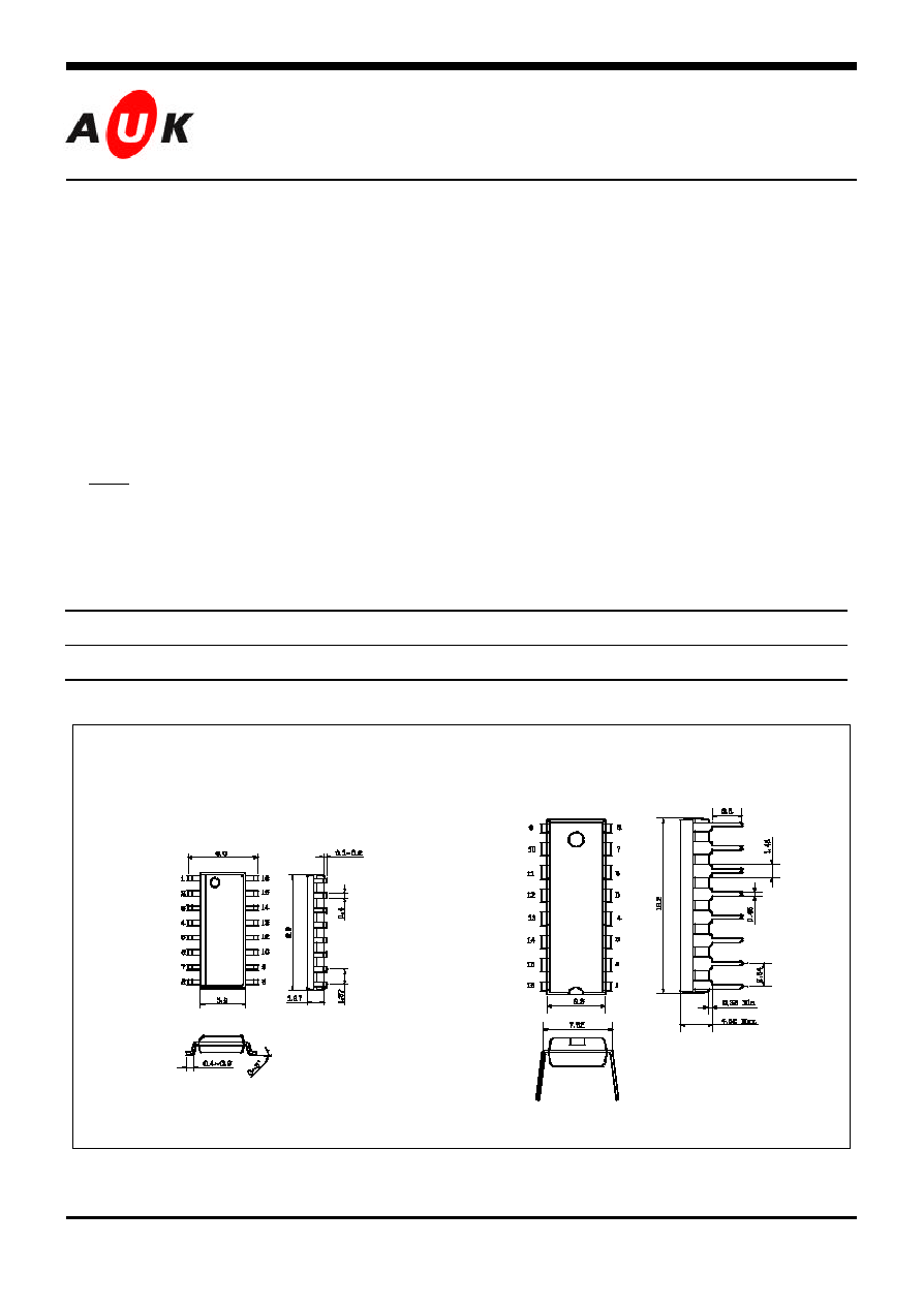
Outline Dimensions unit :
mm
S
S
e
e
m
m
i
i
c
c
o
o
n
n
d
d
u
u
c
c
t
t
o
o
r
r
SOP16
DIP16

KSI-W011-000
2
Absolute Maximum Ratings
(Ta = 25
∞
C)
Characteristic
Symbol
Rating
Unit
Line Voltage
V
L
12
V
Line Current
I
L
140
mA
Power Dissipation
P
D
666
mW
Operating Temperature
T
opr
-25 ~ +70
∞C
Storage Temperature
T
stg
-40 ~ +125
∞C
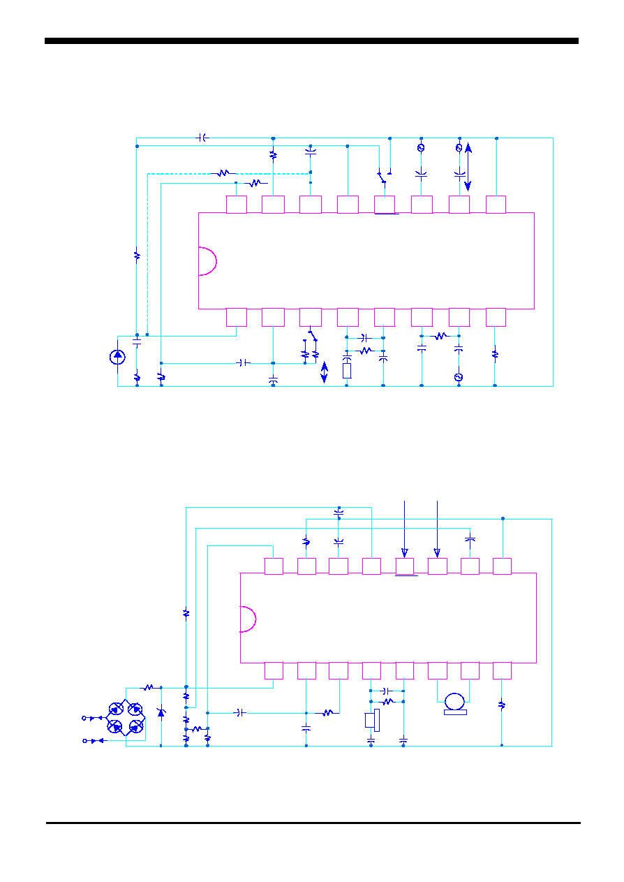
Block Diagram
SL5022/P
13
12
11
10
15
5
4
1
16
2
3
14
8
7
6
9
A t t e n u a t o r
M u t e L o g i c
B i a s
R e f e r e n c e
A G C
L o w V o l t a g e
D T M F
M U T E
R X O
T X G A 1
V
L
S L P E
T X G A 2
R E G
A G C
S T A B
V E E
V c c
M I C -
M I C +
R X I
R x i A m p
M f i A m p
M i c A m p
D T M F A m p
R x A m p
T x A m p
R X G A
KSI-W011-000
3
Pin Description
Pin No.
Symbol
Description
1
VL
Positive power line and TX Amp output
2
TXGA1
TX gain adjustment
3
TXGA2
TX gain adjustment
4
RXO
RX output
5
RXGA
RX gain adjustment
6
MIC
-
MIC(-) input
7
MIC
+
MIC(+) input
8
SRAB
Current stabilizer
9
V
EE
Ground
10
RXI
Rx input
11
DTMF
DTMF signal input
12
MUTE
'H' Mute input
13
V
CC
Internal power supply pin
14
REG
Voltage regulator decoupling
15
AGC
Automation gain control input
16
SLPE
Slope(DC resistance) adjustment
Electrical Characteristics
Characteristics
Symbol
Test Condition
Min.
Typ.
Max.
Unit
ILine = 1mA
ILine = 4mA
-
-
1.6
1.9
-
-
ILine = 15mA
3.55
4
4.25
ILine = 100mA
4.9
5.7
6.5
Line Voltage
V
L
ILine = 140mA
-
-
7.5
V
Variation with
temperature
V
L
/T
ILine = 15mA
-
-0.3
-
mV/k
ILine = 15mA
R
VA
(R
EG
to S
LPE
) = 39K
-
4.5
-
V
Voltage drop over
circuit between
V
L
& V
EE
with external
resistor R
AV
R
VA
ILine = 15mA
R
VA
(V
L
to R
EG
) = 68K
-
3.5
-
V
Ip=1.2mA
2.2
2.7
-
Supply Voltage
V
CC
Mute=High
Ip=0mA
-
3.4
-
V
Between MIC- & MIC+
-
64
-
MIC input impedance
Zi(mic)
MIC- or MIC+ to V-
-
32
-
k
SL5022/P
KSI-W011-000
4
Electrical Characteristics (continued)
Characteristics
Symbol
Test Conditions
Min.
Typ.
Max.
Unit
Common mode
Rejection Ratio
CMRR(Tx)
-
-
82
-
dB
TX Gain
Gv(Tx)
R7=68K, Vin=3mVrms
50.5
52
53.5
dB
TX Gain frequency
Response
G
TXF
f=300 ~ 3400Hz
-
± 0.2
-
dB
DTMF input
impedance
Zi
(MF)
-
-
20.7
-
k
DTMF Gain
G
V(MF)
R7=68K, DTMF mode
24
25.5
27
dB
DTMF Gain Response
G
MF
R7=68K, f=300~3400Hz
-
± 0.2
± 0.5
dB
TX Gain Adjustment
Gv.adj(Tx) R7 = 68k
25k
-12
-8
-7
dB
IL=4mA
-
0.8
-
TX Dynamic output
Voltage
T
O
(Tx)
THD=10%
IL=15mA
1.7
2.3
-
Vrms
TX noise output
Voltage
Vno(Tx)
R7=68K Between
pin6 & pin7=200
-
-69
-
dBmp
RX input impedance
Zi(Rx)
-
-
21
-
K
RX output impedance
Zo(Rx)
-
-
4
-
K
RX Gain
Gv(Rx)
R4=100k, RL=300
29.5
31
32.5
dB
RX Gain Frequency
Response
G
TXF
f=300 ~ 3400Hz
-
± 0.2
-
dB
RL=150
0.22
0.33
-
RX Dynamic output
voltage
Vo
(Rx)
THD=2%
R4=100K
RL=450
0.3
0.48
-
V
RX noise output
voltage
Vno
(Rx)
R
L
=300
R4=100 K
IL= 15mA, Rxi=open
-
50
-
µV
RX Gain adjustment
Gv.adj(Rx) R4=100K
28K
-13
-11
-9
dB
V
IH
(Mute)
-
1.5
-
V
CC
Mute input voltage
V
IL
(Mute)
-
-
-
0.3
V
Mute input current
I
Mute
-
-
8
15
µA
Mute Attenuation
Matt(TX)
MIC+ or MIC- to V
L
(CCIT weighted)
-
70
-
dB
DTMF Gain
Gv(DTMF)
voltage gain from
DTMF to Rxo
-
-19
-
dB
TX Gain variation
range By AGC
G
TXA
R6 = 110k
IL=15mA ~ 70mA
-
-5.8
-
dB
RX Gain variation
range By AGC
G
RXA
R6=110k
IL=15mA ~ 70mA
-
-5.8
-
dB
Highest line current
for maximum gain
I
HL(AGC)
R6=110k
17
23
26
mA
Lowest line current
for minimum gain
I
LL(AGC)
R6=110k
54
61
73
mA
SL5022/P
KSI-W011-000
5
Test Circuit
Application Circuit
SL5022/P
16
15
14
13
12
11
10
9
1
2
3
4
5
6
7
8
S L P E
A G C
R E G
V c c
M U T E
D T M F
I R
V E E
S T A B
M I C +
M I C -
G A R
Q R
G A S 2
G A S 1
L N
SL5022
R V A ( d o w n )
1 0 U
C 7
1 n
V o
C 2
1 0 0 u
R 5
3 . 6 K
C 3
4 . 7 u
R 6
6 8 K
C 4
1 0 0 p
R 4
1 0 0 K
C 1 0
1 0 u
R 7
R n o
2 0 0
C 9
1 0 u
R 1
6 2 0
I
L i n e
1 0 ~ 1 4 0 m A
1 0 0 U
C 1
C 5
1 0 U
V i
V i
R V A ( u p )
C 5
Z L
C 8
1 n
2 5 K
C 6
1 0 0 p
R 9
2 0
6 0 0
V i
BZX79C12
R 1 0
13
t e l e p h o n e
l i n e
16
15
14
13
12
11
10
9
1
2
3
4
5
6
7
8
S L P E
A G C
R E G
V c c
M U T E
D T M F
I R
V E E
S T A B
M I C +
M I C -
G A R
Q R
G A S 2
G A S 1
L N
SL5022
C 7
1n
R 5
3 . 6 K
C 3
4 . 7 u
R 6
C 4
1 0 0 p
R 4
1 0 0 K
R 1
6 2 0
1 0 0 U
C 5
C 8
1n
C 6
1 0 0 p
R 9
20
f r o m d i a l a n d
c o n t r o l c i r c u i t s
1 0 0 U
C 5
R 7
6 8 K
R 2
1 3 0 K
R 3
3 . 9 2 K
R 8
3 9 0
Z b o l
C 2
SL5022
SL5022P
SL5022
SL5022P